Array-based architecture for molecular electronics

a molecular electronics and array technology, applied in the field of molecular electronics, can solve the problems of not teaching how to customize nanoblocks, not knowing how to connect together large numbers of nanoscale or sublithographic devices to create arbitrary logic functions, and not knowing how to arrange for arbitrary connection of logic circuits

Inactive Publication Date: 2006-07-20
CALIFORNIA INST OF TECH +1
View PDF17 Cites 11 Cited by
  • Summary
  • Abstract
  • Description
  • Claims
  • Application Information

AI Technical Summary

Benefits of technology

[0024] A further advantage of the present invention is that the architecture disclosed herein can provide universal logic functionality. The architecture allows a sufficient set of capabilities for performing logic, restoration, routing, and bootstrap programming using only large, crossed wire arrays.
[0025] Additional advantages of the architecture according to the present invention are its minimalism, defect tolerance, and compatibility with emerging, bottom-up, nanoscale fabrication techniques. Furthermore, the disclosed architecture also supports micro-to nanoscale interfacing for communication with conventional integrated circuits and bootstrap loading.

Problems solved by technology

However, the architecture disclosed in Goldstein is restricted to the use of two-terminal devices only and does not teach how nanoBlocks are customized.
It is still not known how to connect together large numbers of these nanoscale or sublithographic devices to create arbitrary logic functions.
Additionally, it is still not known how to arrange for arbitrary connection of (cascading of) logic circuits at the nanoscale level without need for returning to a micro-scale level for signal restoration.
It is also not known how to exploit the limited assembly techniques now possible to build arbitrary logic functions.
It is also not known which logic structures are efficient when dealing with the cost constraints imposed by these fabrication techniques.

Method used


Image

  • Array-based architecture for molecular electronics
  • Array-based architecture for molecular electronics
  • Array-based architecture for molecular electronics

Examples


Embodiment Construction

Basic Passive Devices

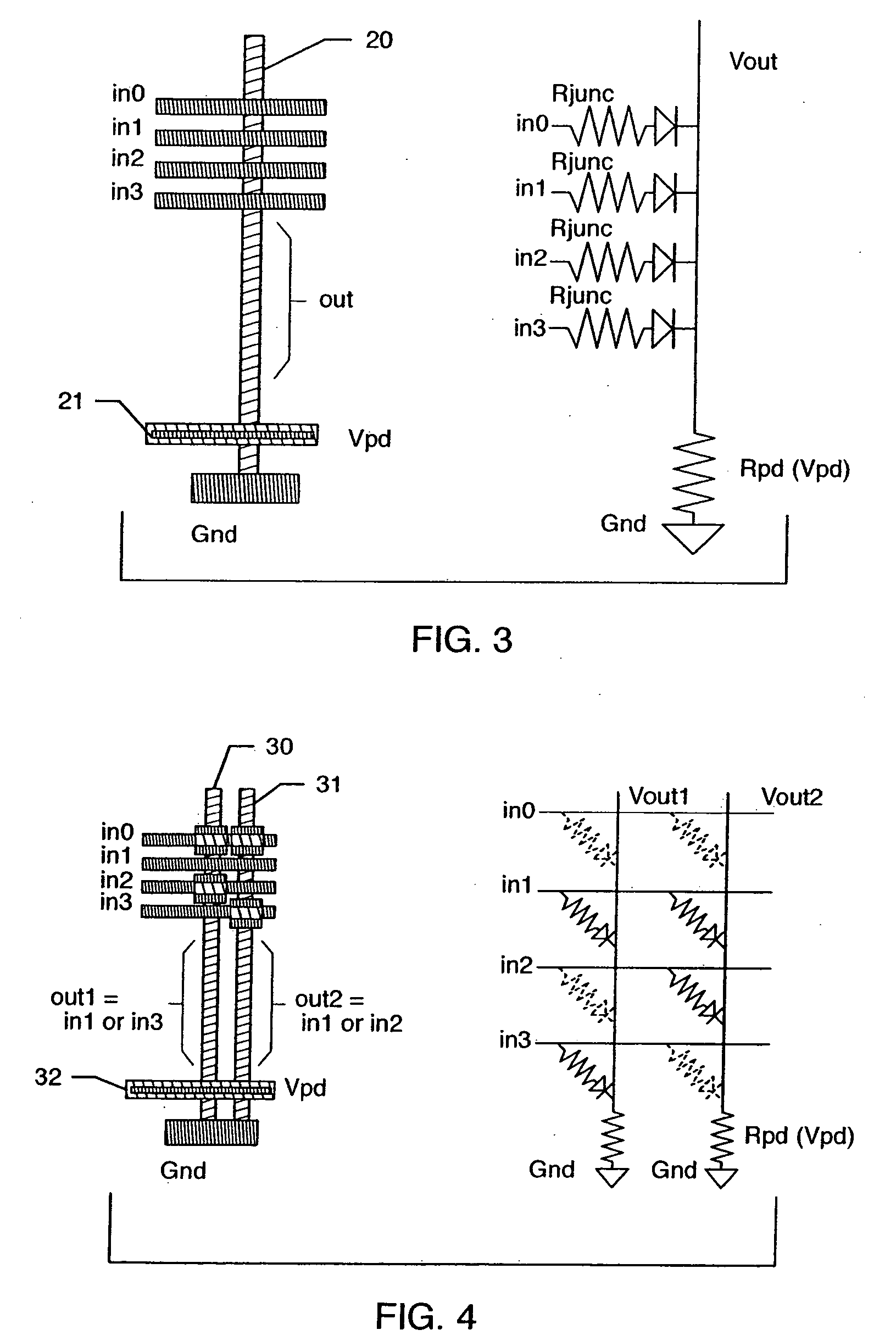
[0039] Reference is initially made to FIG. 3, the left side of which shows a nanotube wired OR logic arrangement. The right side of FIG. 3 shows the electrical equivalent of the left side arrangement. The upper nanotubes or nanowires IN0, IN1, IN2, IN3 contact the lower nanotube 20, thus forming a plurality of low resistance PN-type junctions of the kind already discussed in FIG. 1. In case an upper nanotube IN1 is “far” from the lower nanotube 20, a high impedance configuration is formed. Element 21 is a nanotube covered by oxide, which presents a FET behavior (see FIG. 2), thus producing a voltage-controlled resistance value Rpd. Element 21 acts as a static load in the wired-OR arrangement shown in the Figure.

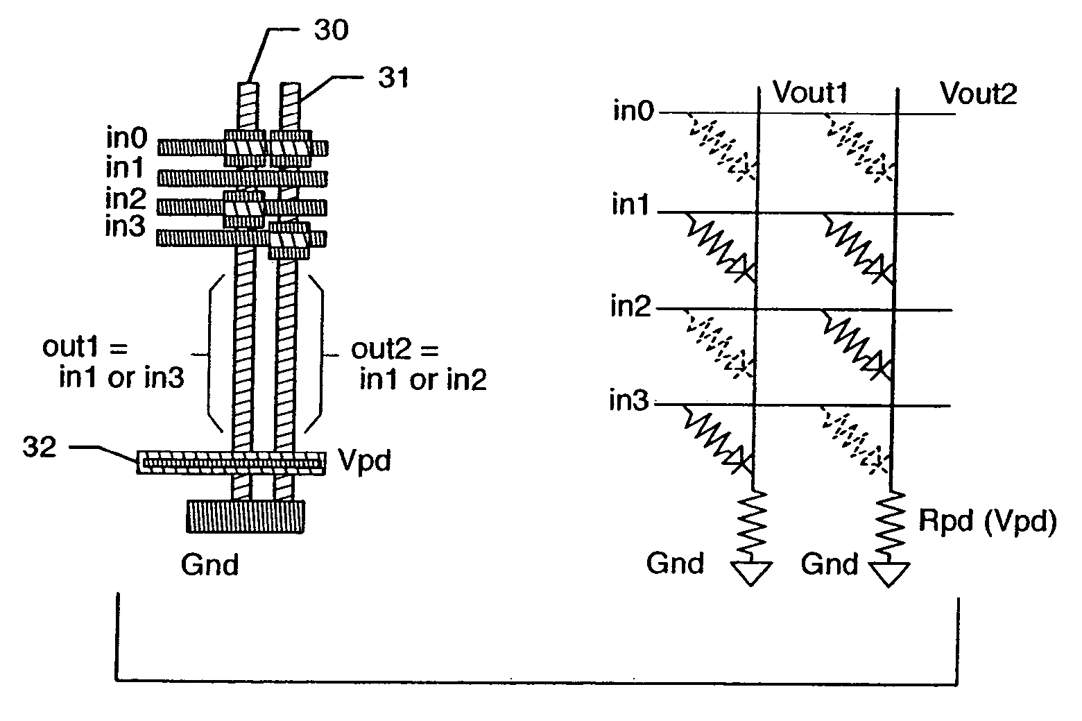
[0040]FIG. 4 shows a programmable diode OR array. As usual, the left side shows the nanotube arrangement, and the right side shows the corresponding electrical equivalent. The black squares between upper nanotubes IN0 . . . IN3 and lower nanotubes 30, ...


PUM


Abstract

An architecture for nanoscale electronics is disclosed. The architecture comprises arrays of crossed nanoscale wires having selectively programmable crosspoints. Nanoscale wires of one array are shared by other arrays, thus providing signal propagation between the arrays. Nanoscale signal restoration elements are also provided, allowing an output of a first array to be used as an input to a second array. Signal restoration occurs without routing of the signal to non-nanoscale wires.

Description

CROSS REFERENCE TO RELATED APPLICATIONS [0001] This application claims the benefit of U.S. provisional Patent Application Ser. No. 60 / 349,561, filed Jan. 18, 2002 for a “Regular architecture for bootstrapping and operation of a universal, molecular-scale computing array” by Andre DeHon and Charles Lieber, the disclosure of which is incorporated herein by reference.STATEMENT REGARDING FEDERALLY SPONSORED RESEARCH OR DEVELOPMENT [0002] The present invention was made with support from the United States Government under Grant number N00014-01-0651 awarded by the Office of Naval Research of the Department of the Navy. The United States Government has certain rights in the invention.BACKGROUND OF THE INVENTION [0003] 1. Field of the Invention [0004] The present invention relates to the field of sublithographic fabrication of electronic circuits, in particular molecular electronics. More specifically, an array-based architecture is disclosed using a collection of techniques where small fea...

Claims


Application Information

Patent Timeline
Patent Type & Authority Applications(United States)
IPC IPC(8): G06F17/50G11C8/10G11C11/34G11C13/02H01L27/28H01L51/00H01L51/05
CPCB82Y10/00G11C8/10G11C13/0023G11C13/003G11C13/025G11C2213/75G11C2213/77G11C2213/81H01L27/28H01L27/285H01L51/0508H01L51/0595H10K19/202H10K19/00H10K10/46H10K10/701
Inventor DEHON, ANDRELIEBER, CHARLES M.
Owner CALIFORNIA INST OF TECH
Why Eureka
Try Eureka