

Semiconductor device
- Summary
- Abstract
- Description
- Claims
- Application Information
AI Technical Summary
Benefits of technology
Problems solved by technology
Method used
Image

Examples
Embodiment Construction
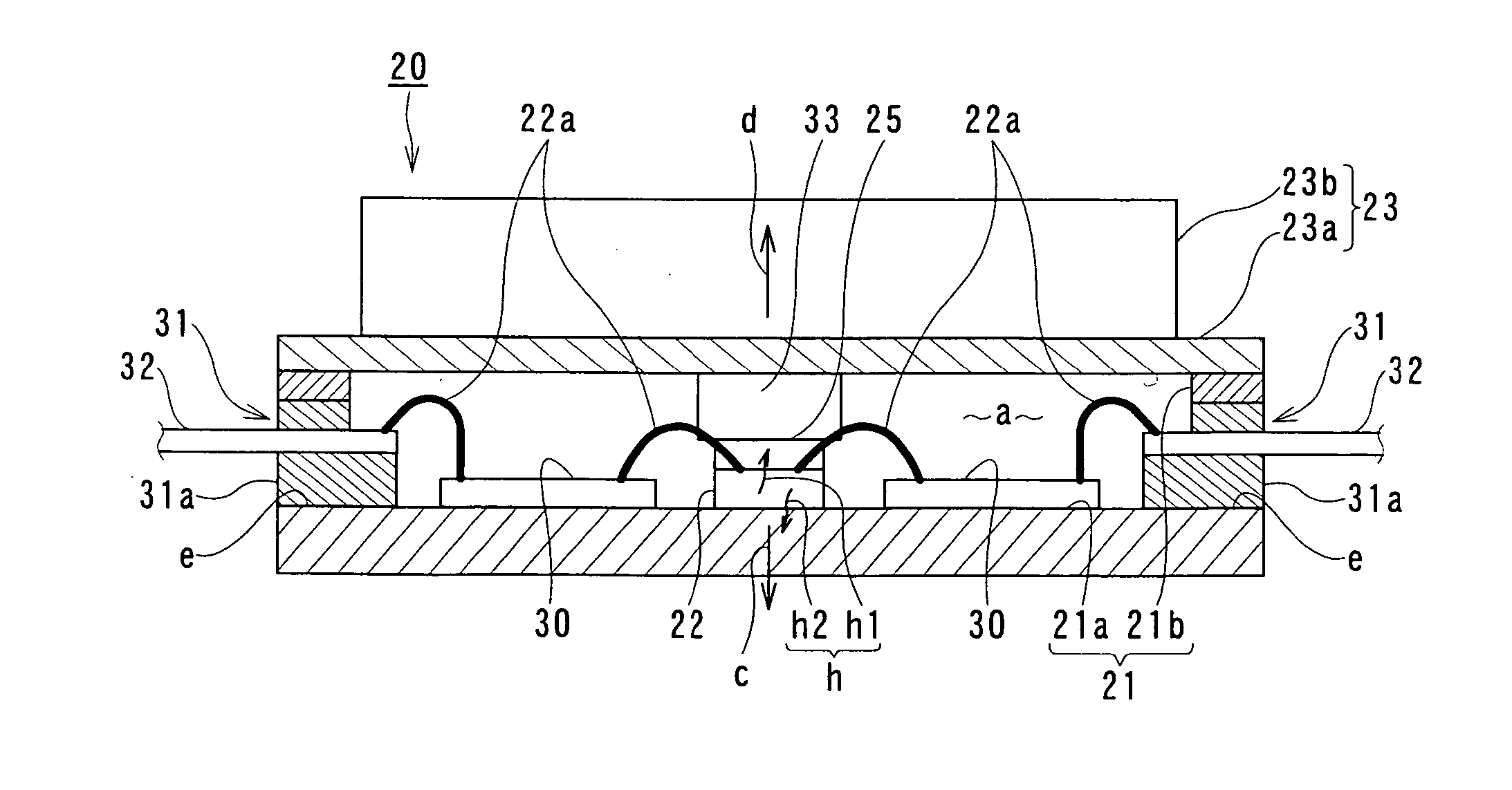
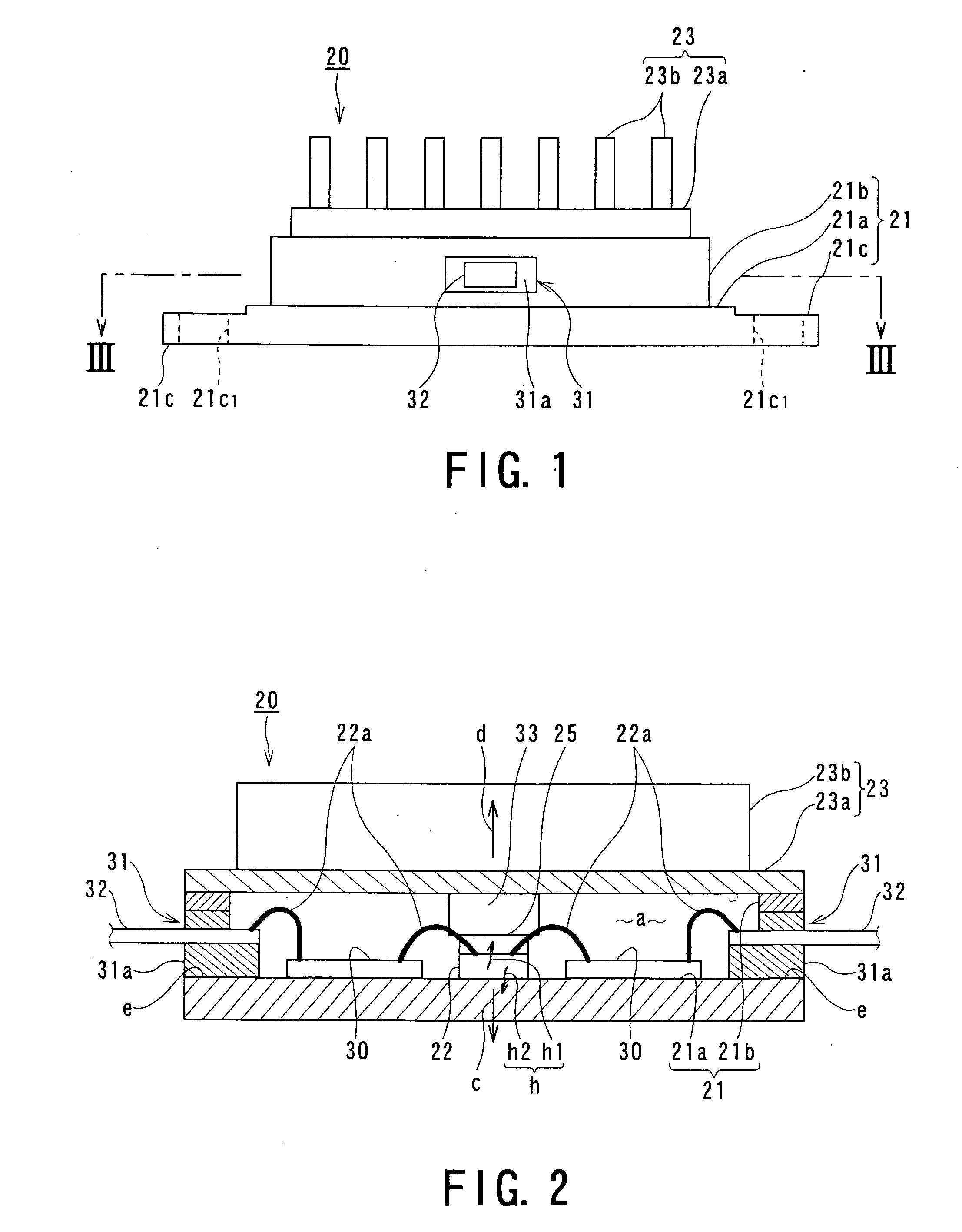
[0032] A semiconductor device according to one embodiment of the present invention will be described with reference to FIGS. 1 to 3.
[0033] This semiconductor device 20 is composed of an envelope 21 used as a base substrate, semiconductor dies (pellets) 22 mounted on this envelope 21 and used as a power element, and a sealing cap 23 covering the semiconductor dies 22 for sealing thereof.
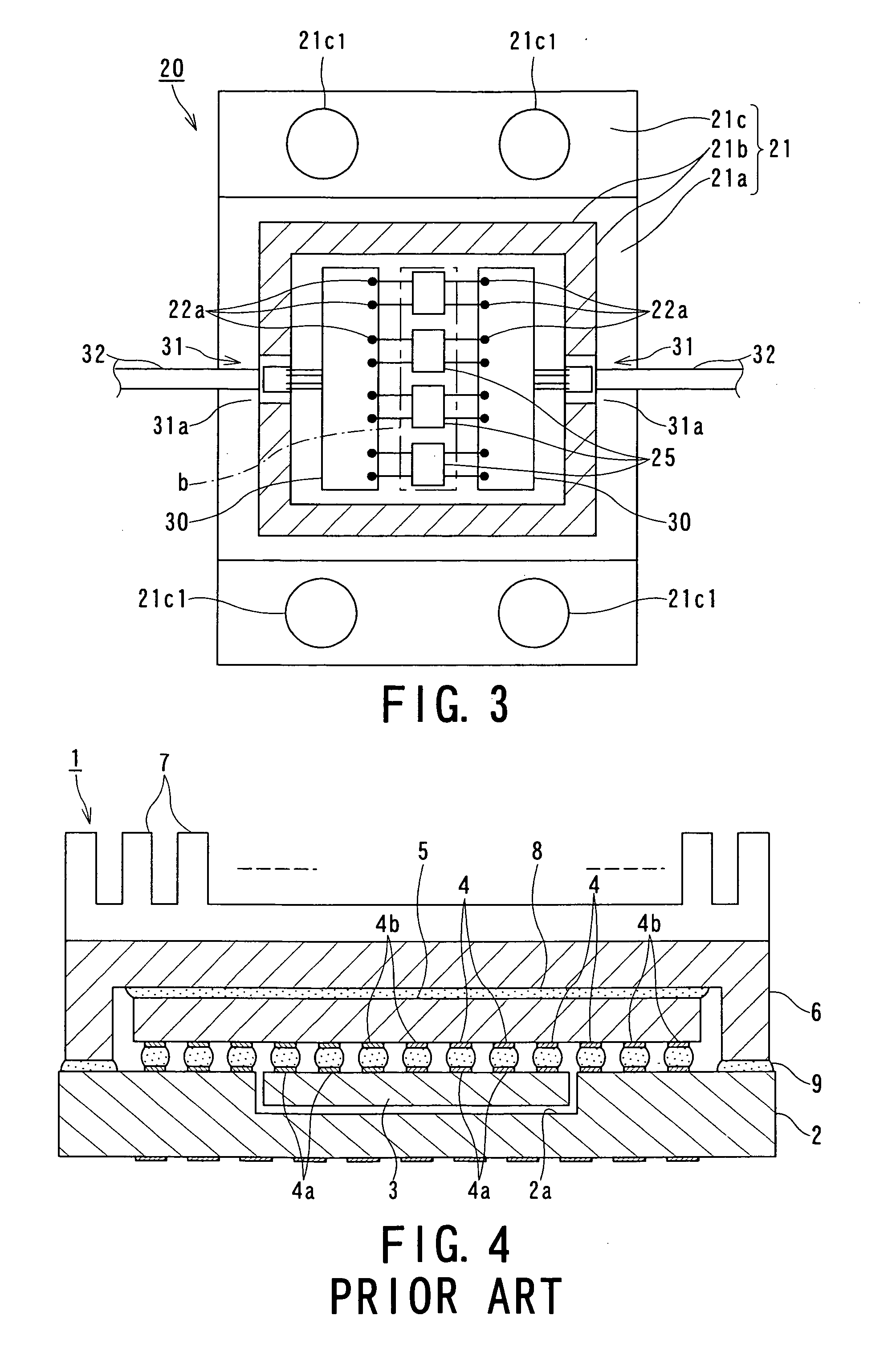
[0034] The envelope 21 is formed of a heat conductive material such as Cu—Mo and, as shown in FIGS. 2 and 3, is composed of a plate portion 21a, a wall portion 21b, and fitting portions 21c, the wall portion 21b being provided along the periphery of the plate portion 21a so as to form a dies receiving portion “a” thereon, the fitting portions 21c being integrally formed with the plate portion 21a so as to protrude outside from the two ends thereof. The fitting portions 21c are each provided with screw holes 21c1 for fixing and are fixed with screws to an apparatus, not shown, on which the semiconduc...
PUM
 Abstract
Description
Claims
Application Information