Semiconductor device

a technology of semiconductor devices and sealing rings, applied in semiconductor devices, semiconductor/solid-state device details, electrical apparatus, etc., can solve the problems of affecting the rigidity and strength of the end parts of the semiconductor device, especially the corner parts, and achieve the effect of preventing the loss of the corner parts of the sealing ring with certainty, improving rigidity and strength, and wide width

Inactive Publication Date: 2006-07-27
NEC ELECTRONICS CORP
View PDF4 Cites 30 Cited by
  • Summary
  • Abstract
  • Description
  • Claims
  • Application Information

AI Technical Summary

Benefits of technology

[0013] In this manner, a load will be applied to the corner parts of the sealing ring at the time of handling the device in the post-processing steps. Since the corner parts of the sealing ring have an improved rigidity and strength as described above, the loss of the corner parts of the sealing ring is prevented with certainty.
[0014] Also, the corner part is formed to have a comparatively large width. Therefore, even if an excessive load is applied to the device and the corner part of the sealing ring is lost together with the substrate, only the outer part of the ...

Problems solved by technology

In these post-processing steps, impact and the like are applied to the separated rectangular semiconductor d...

Method used


Image

  • Semiconductor device
  • Semiconductor device
  • Semiconductor device

Examples


Embodiment Construction

[0026] The invention will be now described herein with reference to illustrative embodiments. Those skilled in the art will recognize that many alternative embodiments can be accomplished using the teachings of the present invention and that the invention is not limited to the embodiments illustrated for explanatory purposed.

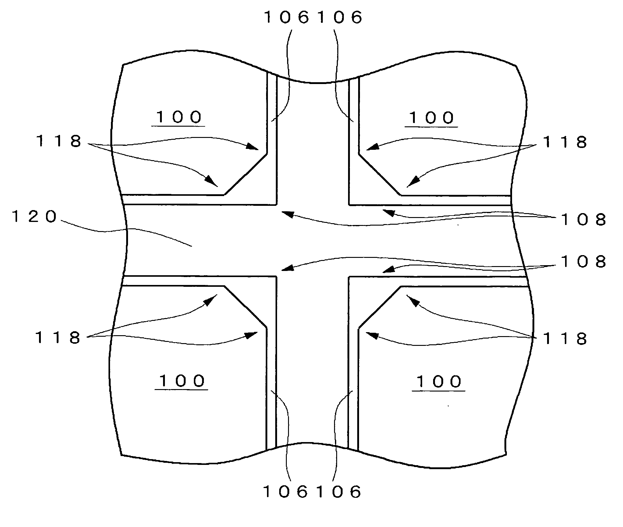
[0027] Hereafter, preferable embodiments of a semiconductor device according to the invention will be described with reference to the attached drawings. In the following embodiments, an example will be described in which a corner part formed to have a larger width in a sealing ring is formed to have a triangular shape in a plan view. Here, in the description of the drawings, the same elements will be denoted with the same symbols, and a duplicated description thereof will not be shown.

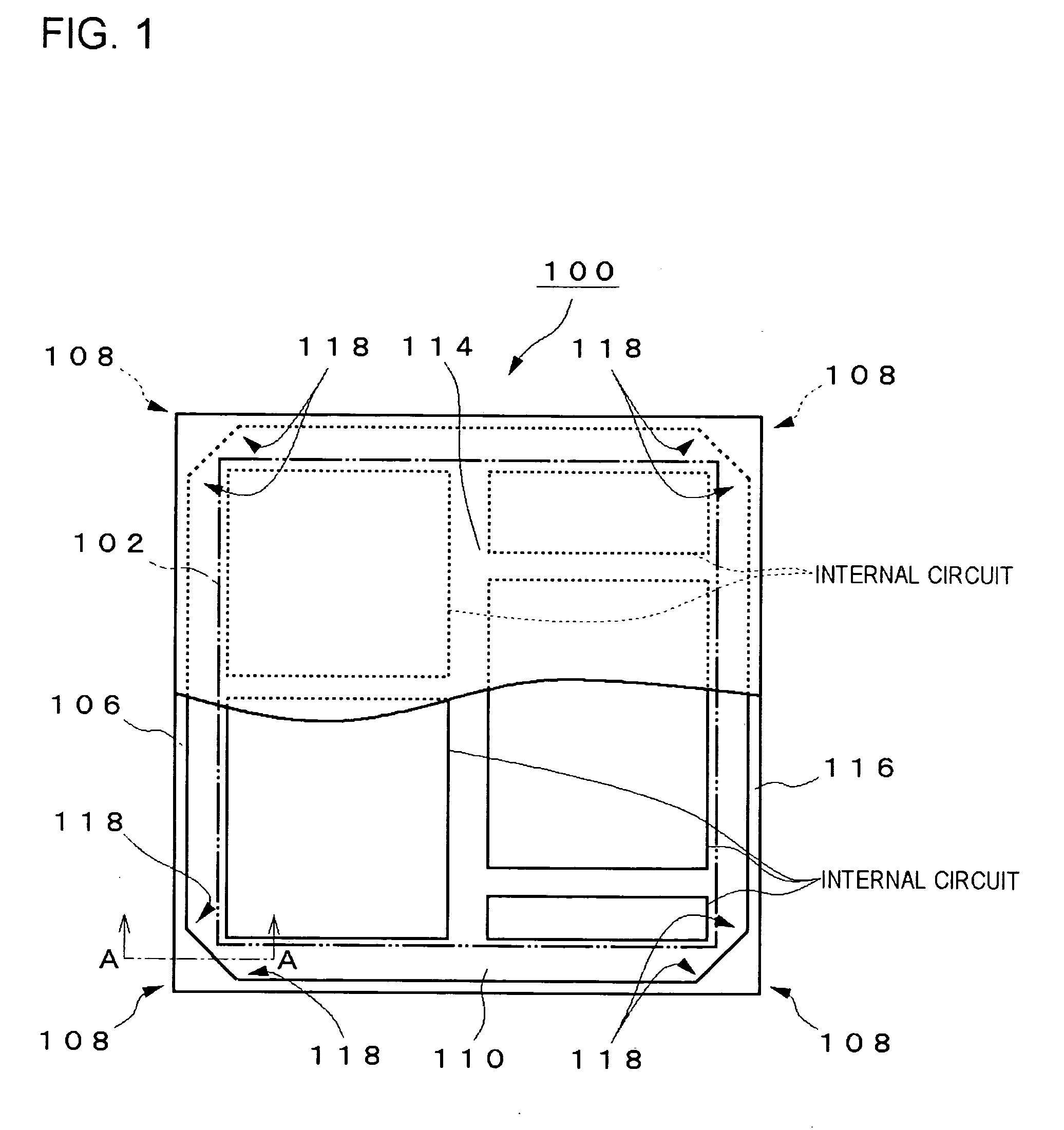
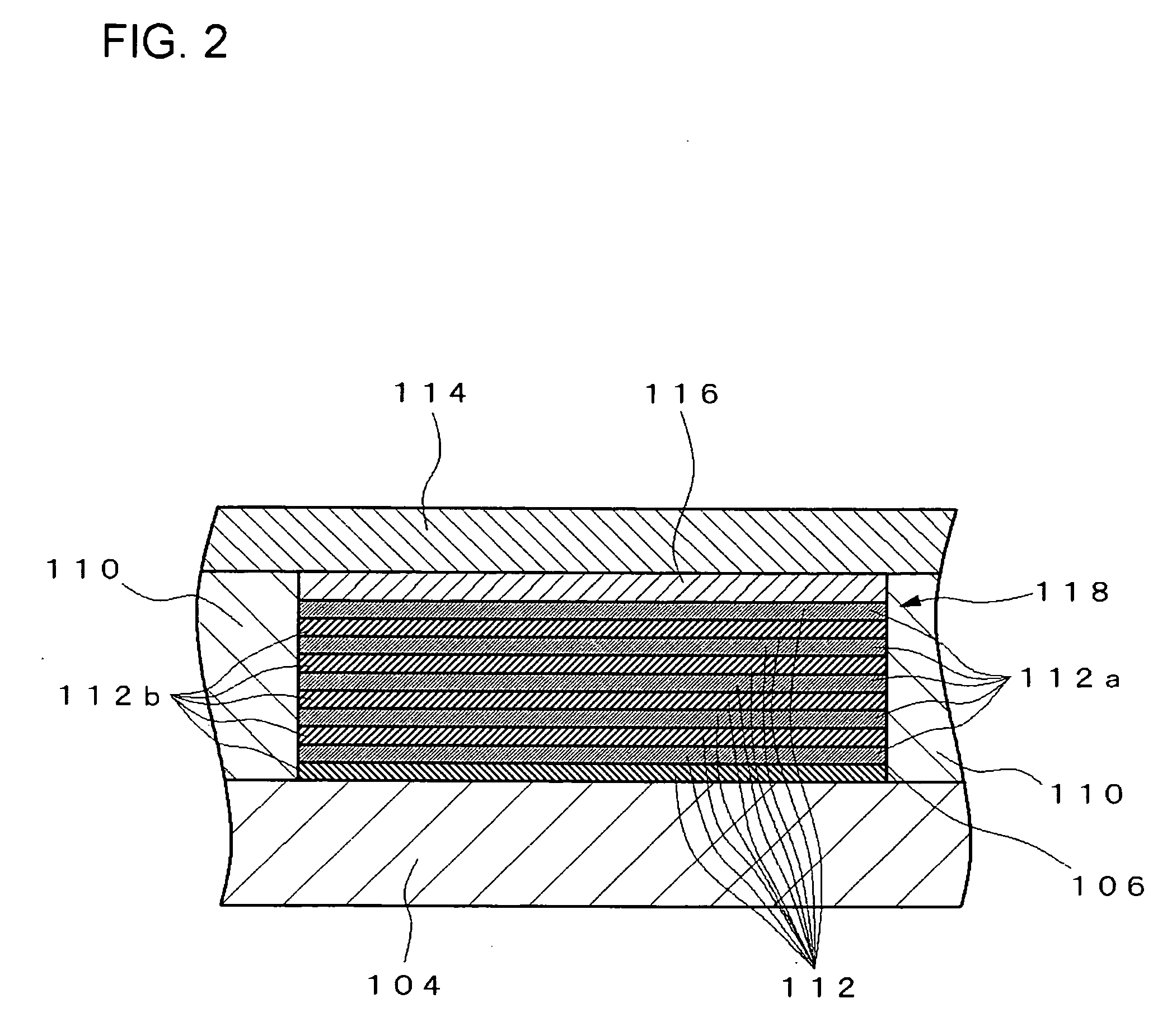
[0028]FIG. 1 is a model plan view of a semiconductor device showing one embodiment of the invention. FIG. 2 is a cross-sectional view taken along the line A-A of FIG. 1.

[0029] R...


PUM


Abstract

A semiconductor device is provided with a sealing ring 106 made of a metal which surrounds an integrated circuit part 102 and which is formed on a substrate 104 along an outer perimeter of the rectangular device. At least one corner part 108 of the sealing ring is formed to have a larger width than other parts of the sealing ring 106, so as to increase the rigidity and the strength of the corner part of the sealing ring 106. Thus, the strength of the corner part of the sealing ring is improved. Also, even if the corner part of the sealing ring is lost, the penetration of moisture into the integrated circuit side is inhibited.

Description

[0001] This application is based on Japanese Patent application NO. 2005-017483, the content of which is incorporated hereinto by reference. BACKGROUND [0002] 1. Technical Field [0003] The present invention relates to a semiconductor device provided with a sealing ring which is formed on a substrate along an outer perimeter of the device. [0004] 2. Related Art [0005] A semiconductor device has a substrate on which numerous circuit elements are formed, and is constructed by interconnecting the circuit elements so as to perform predetermined operations, functions, and the like. In recent years, semiconductor devices are highly integrated, and the circuit elements and the interconnects are reduced in scale, so that the pitch of the interconnects tends to be smaller. When the pitch of the interconnects becomes small, the interconnect resistance increases, thereby necessitating adoption of copper interconnect lines having a low resistivity and insulating interlayers having a low dielectr...

Claims


Application Information

Patent Timeline
IPC IPC(8): H01L23/12
CPCH01L23/562H01L23/585H01L2924/0002H01L2924/00H01L21/3205
Inventor HIRATA, SHINYA
Owner NEC ELECTRONICS CORP
Why Eureka
Try Eureka