Integrated transformer structure and method of fabrication

a transformer and integrated technology, applied in the field of integrated transformer structure, can solve the problems of large ohmic loss, inductors that require extra space, and are difficult to provide in high-density circuit board fabrication

Active Publication Date: 2006-08-03
INTEL CORP
View PDF9 Cites 69 Cited by
  • Summary
  • Abstract
  • Description
  • Claims
  • Application Information

AI Technical Summary

Problems solved by technology

These interconnects have high impedances and result in large ohmic losses.
Also, discrete inductors require extra space outside the chip package, which is difficult to provide for in high-density circuit board fabrication.
The first drawback of spiral inductors includes the large area necessary to create large inductances.
Another drawback of spiral inductors includes the tendency of the inductors to have high resistances.
This high resistance deteriorates the quality factor of the inductors, making them too lossy for such applications as power delivery.
Furthermore, spiral inductors force the magnetic flux into the silicon substrate, causing both eddy current losses and interference with devices.

Method used


Image

  • Integrated transformer structure and method of fabrication
  • Integrated transformer structure and method of fabrication
  • Integrated transformer structure and method of fabrication

Examples


Embodiment Construction

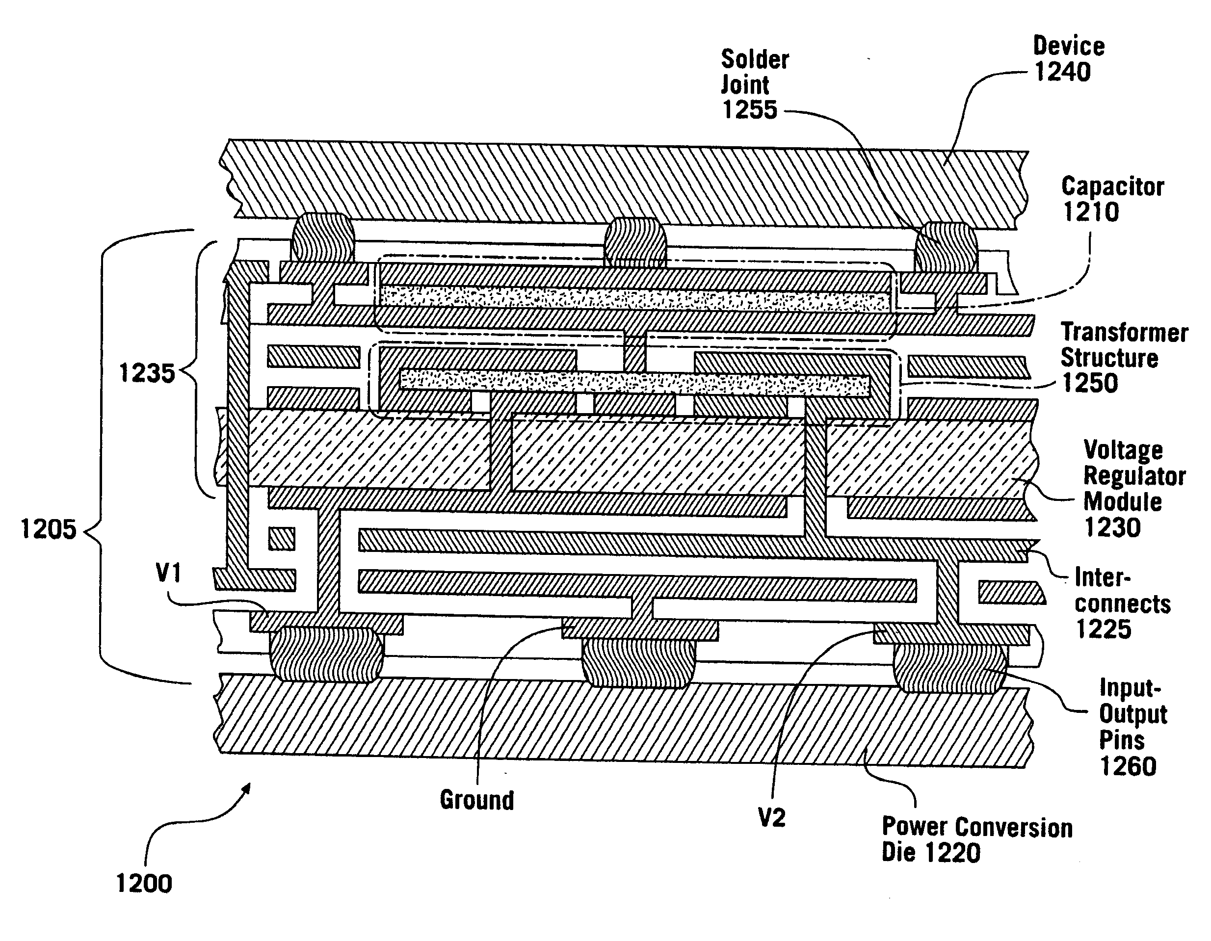
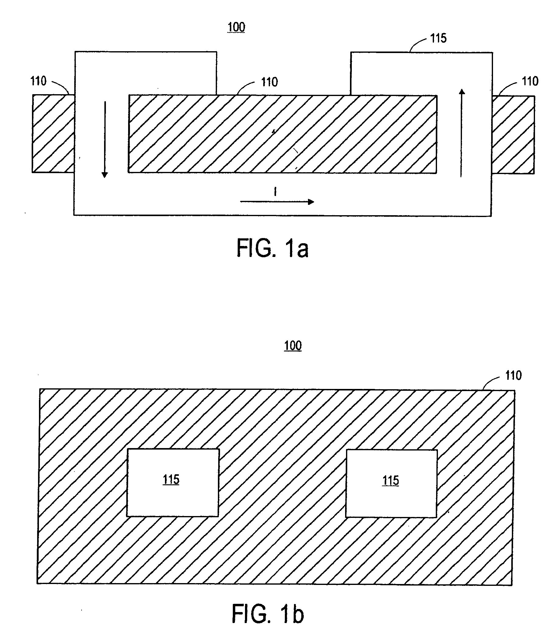
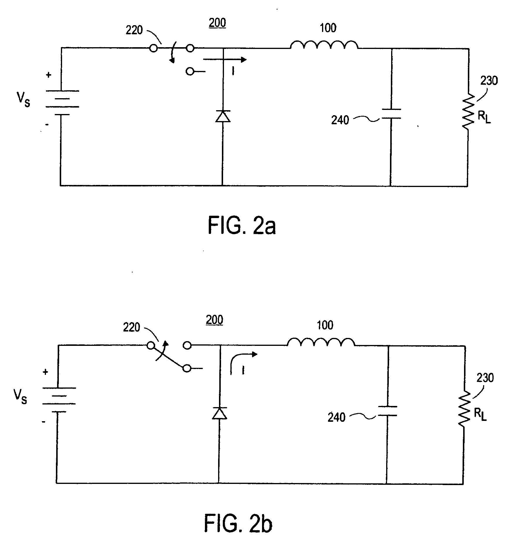
[0031] An embodiment of the present invention is an integrated transformer structure (as shown in FIGS. 7-12) and its method of fabrication using integrated inductor structure 100 (as shown in FIG. 1a). In an embodiment, the integrated inductor structure 100, as shown in FIG. 1a and FIG. 1b, is a solenoid structure115 with a single-turn that is filled with and is surrounded by magnetic material 110. The magnetic material 110 enables a reduction of the inductor size because the magnetic material 110 has a relative magnetic permeability greater than one. This results in a higher inductance per area than an inductor without magnetic material. In an embodiment of the inductor structure 100, the area can be about 0.01-9 mm2 with an inductance in the nanohenry (nH) range. The dimensions of the structure of the inductor can be altered to meet specific inductance and area requirements.

[0032] Another benefit of the magnetic material 110 is the encapsulation of the magnetic flux within the p...


PUM

PropertyMeasurementUnit
ferromagnetic resonance frequencyaaaaaaaaaa
areaaaaaaaaaaa
inductanceaaaaaaaaaa

Abstract

A microelectronic assembly including a die substrate, a plurality of electronic components formed in and on the die substrate and connected to one another to form an integrated circuit, a first and a second single-turn inductor, and a magnetic material electro-magnetically coupling the first and the second single-turn inductor to one another to form a transformer, the transformer being connected to the integrated circuit.

Description

BACKGROUND [0001] 1. Field of the Disclosure [0002] The present disclosure relates to the field of semiconductor devices and more specifically to an integrated transformer structure and its method of fabrication. [0003] 2. Discussion of Related Art [0004] The need for transformers in semiconductor design dictates the use of discrete inductors or spiral inductors. The discrete inductor is in an off-chip, off-package configuration and requires long interconnects to connect the inductor to a chip. These interconnects have high impedances and result in large ohmic losses. Also, discrete inductors require extra space outside the chip package, which is difficult to provide for in high-density circuit board fabrication. [0005] Spiral inductors are created through windings of metal thin films, usually on a semiconductor substrate. The first drawback of spiral inductors includes the large area necessary to create large inductances. Another drawback of spiral inductors includes the tendency o...

Claims


Application Information

Patent Timeline
Patent Type & Authority Applications(United States)
IPC IPC(8): H01F27/28
CPCH01F17/0006H01L2224/16235H01F27/2804H01F41/046H01L23/49822H01L23/49833H01L23/49838H01L2224/16H01L2924/01077H01L2924/01078H01L2924/15312H01L2924/3011H01L23/645H01L2924/01019H01F19/04H01L2224/16265H01L2924/00014H01L2924/00011H01L2224/0401
Inventor BRAUNISCH, HENNING
Owner INTEL CORP
Why Eureka
Try Eureka