Substrate structure with embedded semiconductor chip and fabrication method thereof

Active Publication Date: 2006-08-10
PHOENIX PRECISION TECH CORP
View PDF8 Cites 19 Cited by
  • Summary
  • Abstract
  • Description
  • Claims
  • Application Information

AI Technical Summary

Benefits of technology

[0010] In the structure and fabrication method of substrate with embedded semiconductor chip of the present invention, the size of the opening of the first surface of the carrier board is greater than the size of the to-be-embedded semiconductor chip, and only a portion of the opening of the first surface communicates with the opening of the second surface, so that the first open

Problems solved by technology

However, current BGA structure can not meet the electrical and heat spreading requirements under the circumstances of more pins (1500 pin) and high frequency (5 GHz).
FCBGA structure can be used in products having said more pins and high frequency, however, whose package cost is high, and there are many limitations in this technology, especially in the electrically connecting portion thereof, for the sake of environment protection, electrically connecting materials

Method used


Image

  • Substrate structure with embedded semiconductor chip and fabrication method thereof
  • Substrate structure with embedded semiconductor chip and fabrication method thereof
  • Substrate structure with embedded semiconductor chip and fabrication method thereof

Examples


Example

[0015] The following embodiments are used to describe the present invention; those skilled in the art can easily understand other advantages and functions of the present invention via the contents disclosed in the description. Various embodiments can be employed in the present invention; and the detail of the description can be based on and employed in various points of view, which can be modified within the scope of the present invention.

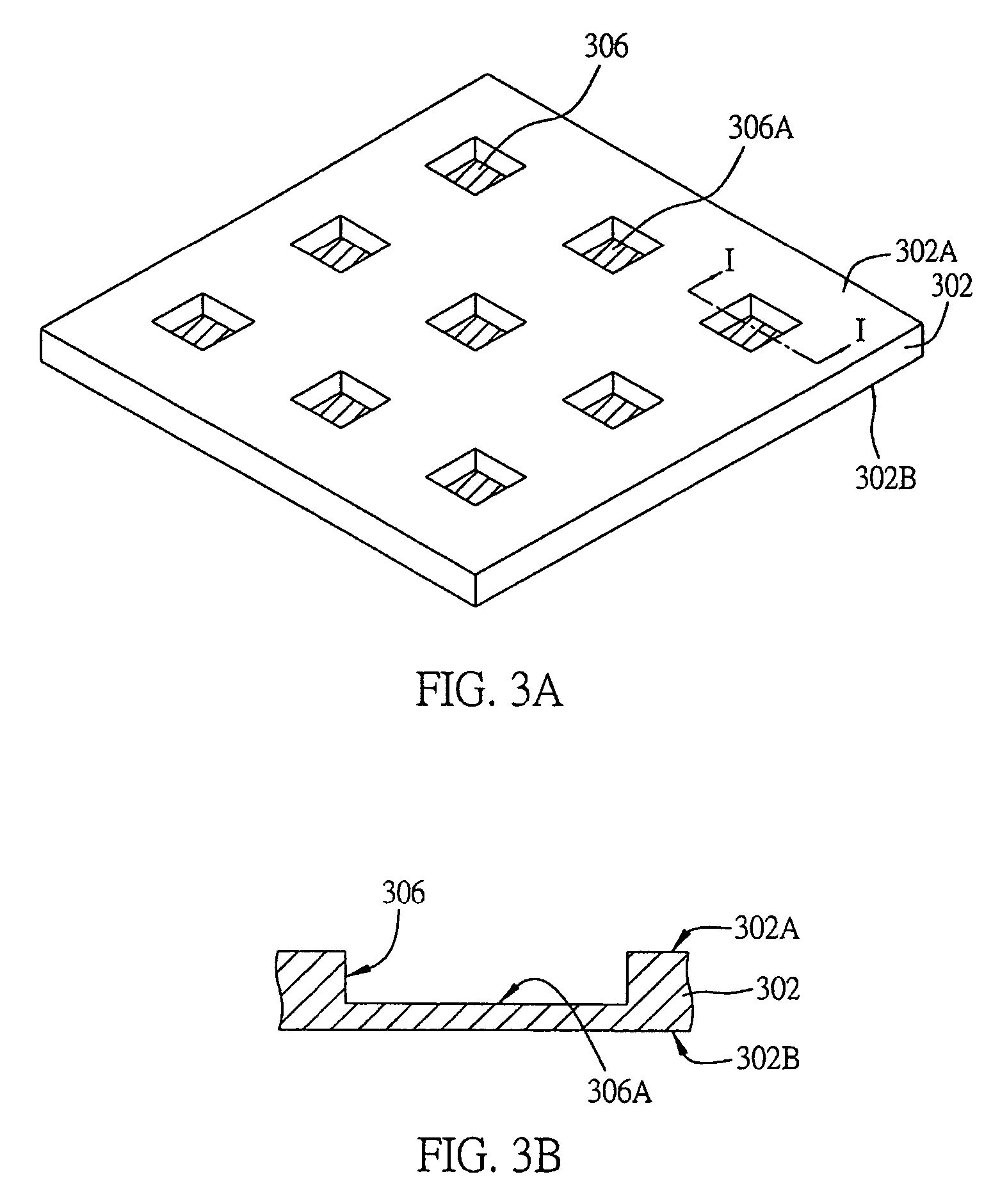
[0016]FIG. 3A to FIG. 3H are flow charts showing the fabrication method of the semiconductor package of the present invention.

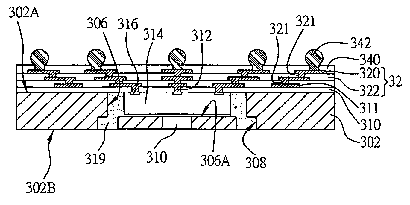
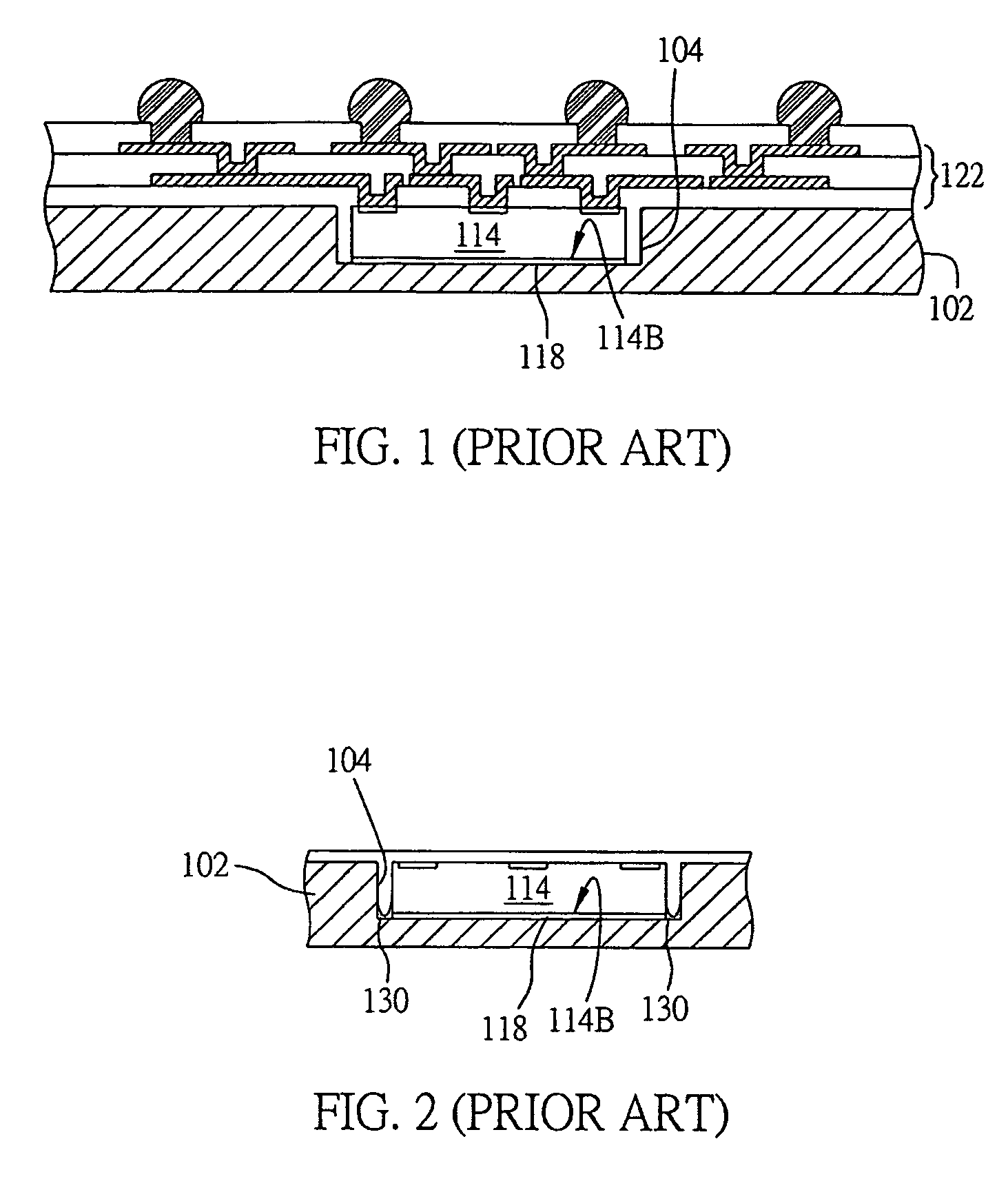
[0017] Firstly, referring to FIG. 3A, a carrier board 302 having a first surface 302A and a second surface 302B is provided, a first opening 306 having a predetermined depth while not running through the carrier board 302 is defined in the first surface 302A of the carrier board 302. FIG. 3B is a section view along I-I line cutting the carrier board 302 having the first opening 306, wherein a mounting surface 306A is forme...


PUM


Abstract

A substrate structure with embedded semiconductor chip and a fabrication method thereof are provided. The method includes: providing a carrier board having a first surface and an opposing second surface, wherein a first opening and an opposing second opening are formed in the first and second surfaces respectively, and a portion of the first opening communicates with the second opening; mounting at least one semiconductor chip to bottom of the first opening to be received in the first opening; filling an adhesive material in the first and second openings and in a gap between the chip and the carrier board to adhere the chip; forming a dielectric layer on the carrier board and the chip; and forming a circuit layer on the dielectric layer and forming conductive structures in the dielectric layer, so that the circuit layer is electrically connected to the chip via the conductive structures.

Description

FIELD OF THE INVENTION [0001] The present invention relates to a structure and fabrication method of a semiconductor package, particularly, and more specifically, to a package structure and fabrication method of substrate with embedded semiconductor chip. BACKGROUND OF THE INVENTION [0002] With the development of semiconductor package technology, various package types are developed for semiconductor devices, wherein a semiconductor chip is firstly mounted on a package substrate or a conductive wire frame, the semiconductor chip is electrically connected to the package substrate of the conductive wire frame, and then an encapsulant is employed to encapsulate. Ball grid array (BGA) is an advanced semiconductor package technology, whose feature is to employ a package substrate to mount the semiconductor chip, wherein self-alignment technology is employed to mount a plurality of solder balls to the back surface of the package substrate, so as to accommodate more I / O connections on a sem...

Claims


Application Information

Patent Timeline
IPC IPC(8): H01L23/02H01L21/48
CPCH01L23/49816H01L23/5389H01L2224/04105H01L2224/20H01L2224/24227H01L2924/15153H01L2924/15165H01L2924/15174H01L2924/15311H01L2224/32245H01L2224/73267
Inventor HSU, SHIH-PING
Owner PHOENIX PRECISION TECH CORP
Why Eureka
Try Eureka