Semiconductor light emitting device and method of manufacture

a technology of semiconductors and light emitting devices, which is applied in the direction of light and heating equipment, other domestic objects, optical articles, etc., can solve the problems of significant drop in the light output of led devices, thermal and photo degradation of epoxy-based encapsulating materials, and relatively elaborate problems

Inactive Publication Date: 2006-08-24
AVAGO TECH INT SALES PTE LTD
View PDF11 Cites 68 Cited by
  • Summary
  • Abstract
  • Description
  • Claims
  • Application Information

AI Technical Summary

Problems solved by technology

However epoxy-based encapsulating materials suffer from thermal and photo degradation.
Degradation of the encapsulant results in increased absorption of light in the blue to green wavelengths, causing a “yellowing” effect on clear epoxy encapsulant and redu

Method used


Image

  • Semiconductor light emitting device and method of manufacture
  • Semiconductor light emitting device and method of manufacture
  • Semiconductor light emitting device and method of manufacture

Examples


Embodiment Construction

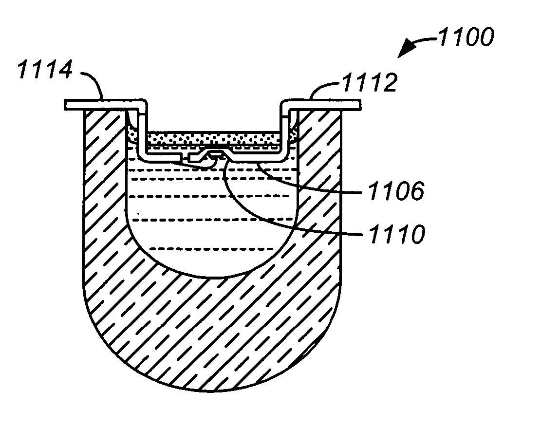
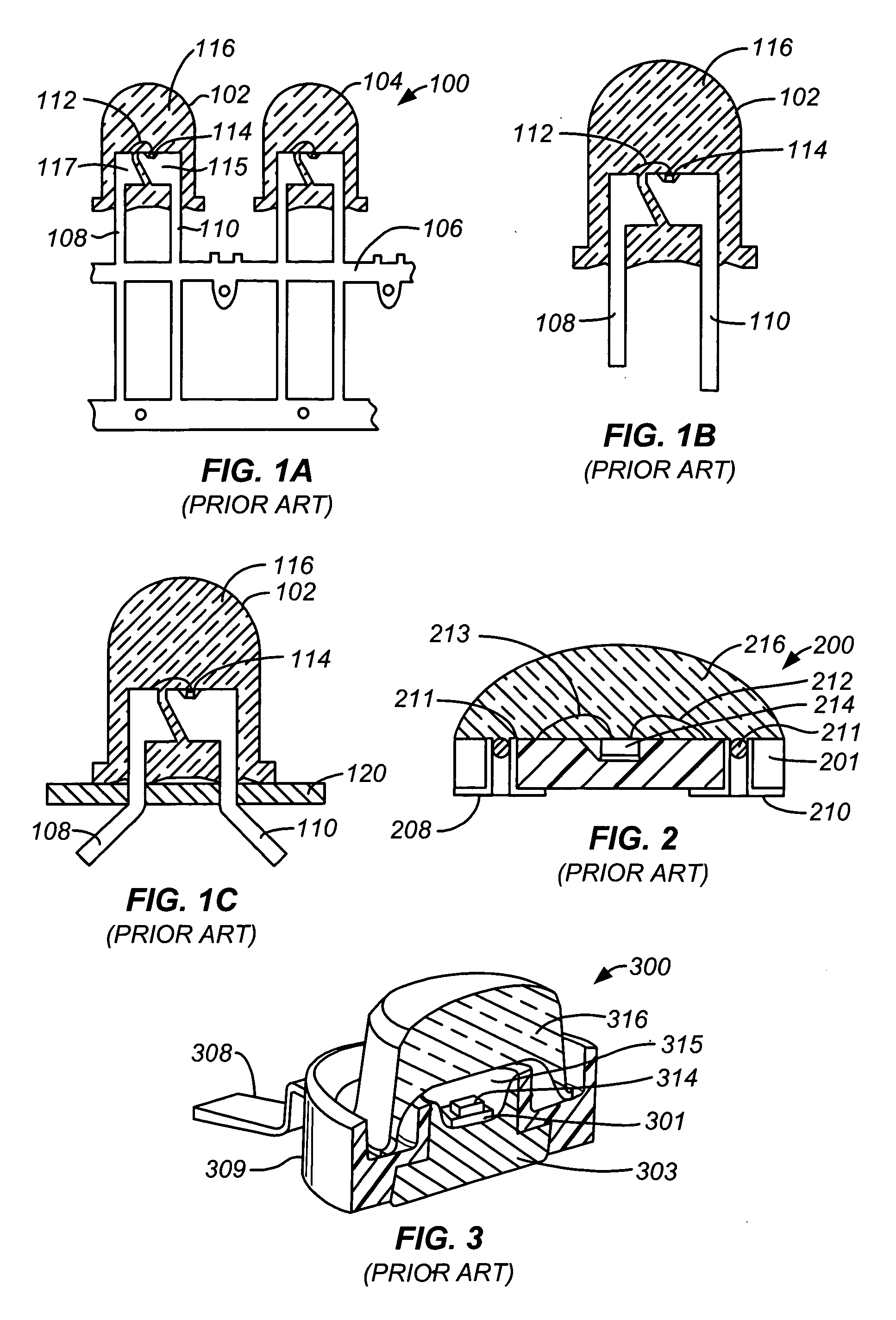
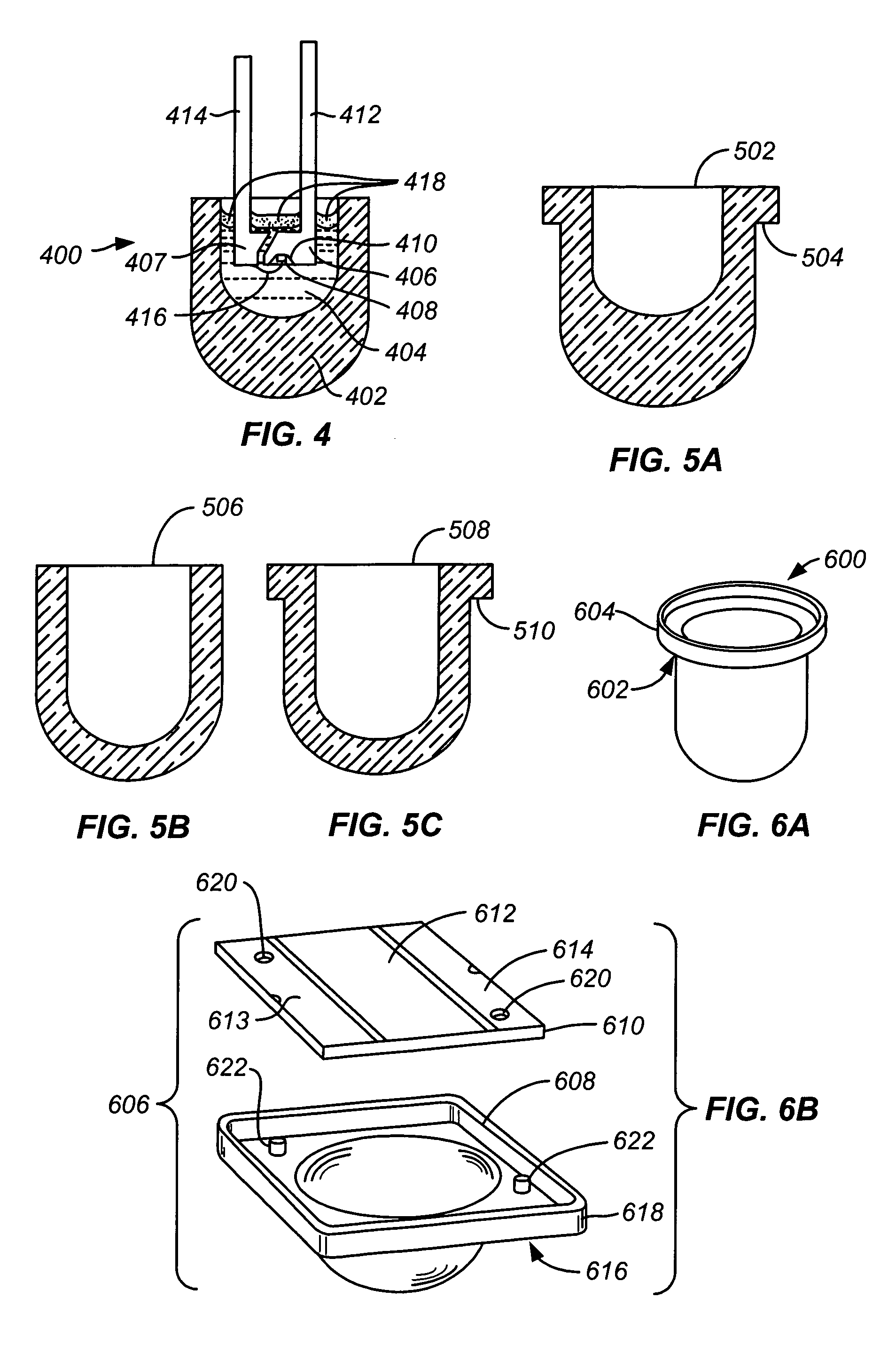
[0033] Silicone elastomers offer desirable characteristics as an encapsulation material. Silicone elastomers offer high thermal stability, low photo-degradation, low light loss transmission characteristics, a wide range of refractive indices, low stress after encapsulation cure, and low cost. They are non-toxic and are not sensitive to high humidity high temperature environments. Silicone encapsulants are particularly desirable for use with light emissions with a wavelength ranging from 200 nm to 570 nm because of the low transmission loss, and more particularly when used in high-temperature operations (i.e. up to 100° C.).

[0034] However, a cured silicone encapsulant typically has a hardness of less than Durometer Shore 70A. The silicone polymer may be liquid, gelatinous or in solid state under various stages of manufacturing. However the low hardness of silicone polymer has the disadvantages of low resistance to scratches, abrasion and wear. Furthermore, packages formed from silic...


PUM

PropertyMeasurementUnit
Poweraaaaaaaaaa
Wavelengthaaaaaaaaaa

Abstract

A light-emitting diode (“LED”) device has an LED chip attached to a substrate. The terminals of the LED chip are electrically coupled to leads of the LED device. Elastomeric encapsulant within a receptacle of the LED device surrounds the LED chip. A second encapsulant is disposed within an aperture of the receptacle on the elastomeric encapsulant.

Description

CROSS-REFERENCE TO RELATED APPLICATIONS [0001] Not applicable. STATEMENT REGARDING FEDERALLY SPONSORED RESEARCH OR DEVELOPMENT [0002] Not applicable. REFERENCE TO MICROFICHE APPENDIX [0003] Not applicable. BACKGROUND OF THE INVENTION [0004] A conventional light emitting diode (“LED”) device uses an epoxy as encapsulating material. The encapsulation process is frequently accomplished by injection molding, transfer molding or casting. Cured epoxy encapsulant has relatively high hardness, which provides resistance to scratches and abrasion, high rigidity, and high initial light transmissivity. Conventional encapsulated LED devices come in a variety of sizes and styles, such as 4 mm Oval LED Lamps, 5 mm Round LED Lamps, Chip LEDs and plastic leaded chip carriers (“PLCCs”). [0005] However epoxy-based encapsulating materials suffer from thermal and photo degradation. Degradation is especially acute if the wavelength emitted by the LED chip is in the near the ultraviolet (“UV”) portion of ...

Claims


Application Information

Patent Timeline
IPC IPC(8): H01L29/22F21K99/00H01L33/56
CPCB29C33/0016B29C35/02H01L2924/12041H01L33/60H01L33/52B29C39/006B29K2021/00B29K2995/0018B29L2011/00H01L33/56H01L24/97H01L2224/48091H01L2224/48247H01L25/0753H01L33/50H01L2924/00014H01L2924/00H01L2924/351H01L2924/15787
Inventor CHEW, TONG FATT
Owner AVAGO TECH INT SALES PTE LTD
Why Eureka
Try Eureka