Organic EL panel

Active Publication Date: 2006-08-31
SANYO ELECTRIC CO LTD
View PDF21 Cites 36 Cited by
  • Summary
  • Abstract
  • Description
  • Claims
  • Application Information

AI Technical Summary

Benefits of technology

[0012] Hence, in the present invention, the microcavity effect of enhancing the light of a specific wavelength can be changed or

Problems solved by technology

However, the organic EL element includes an organic layer that tends to deteriorate depe

Method used


Image

  • Organic EL panel
  • Organic EL panel
  • Organic EL panel

Examples


first embodiment

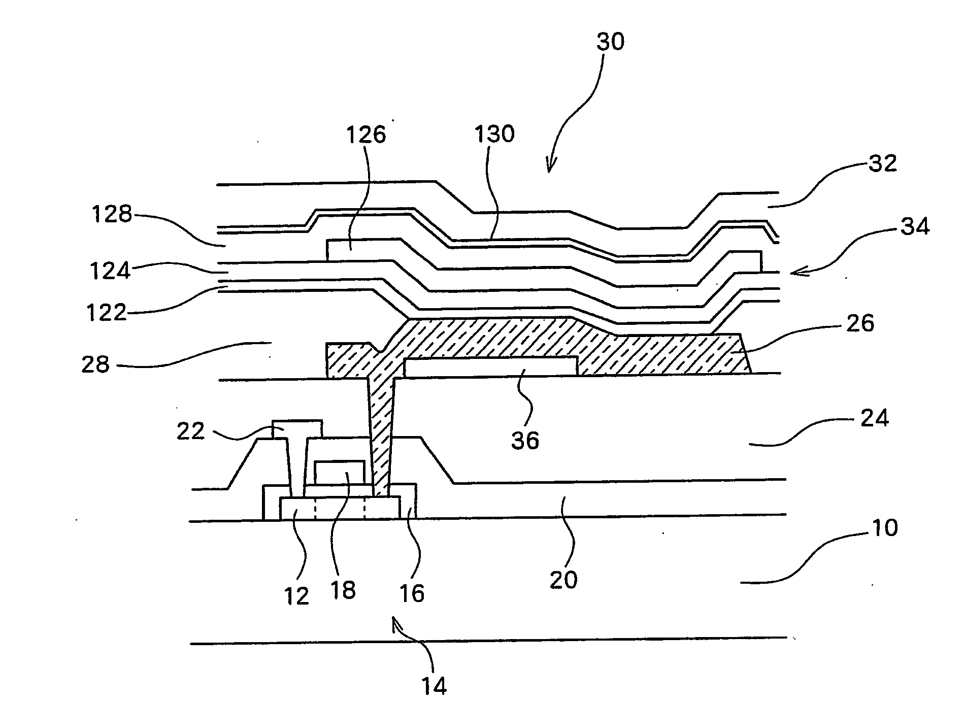
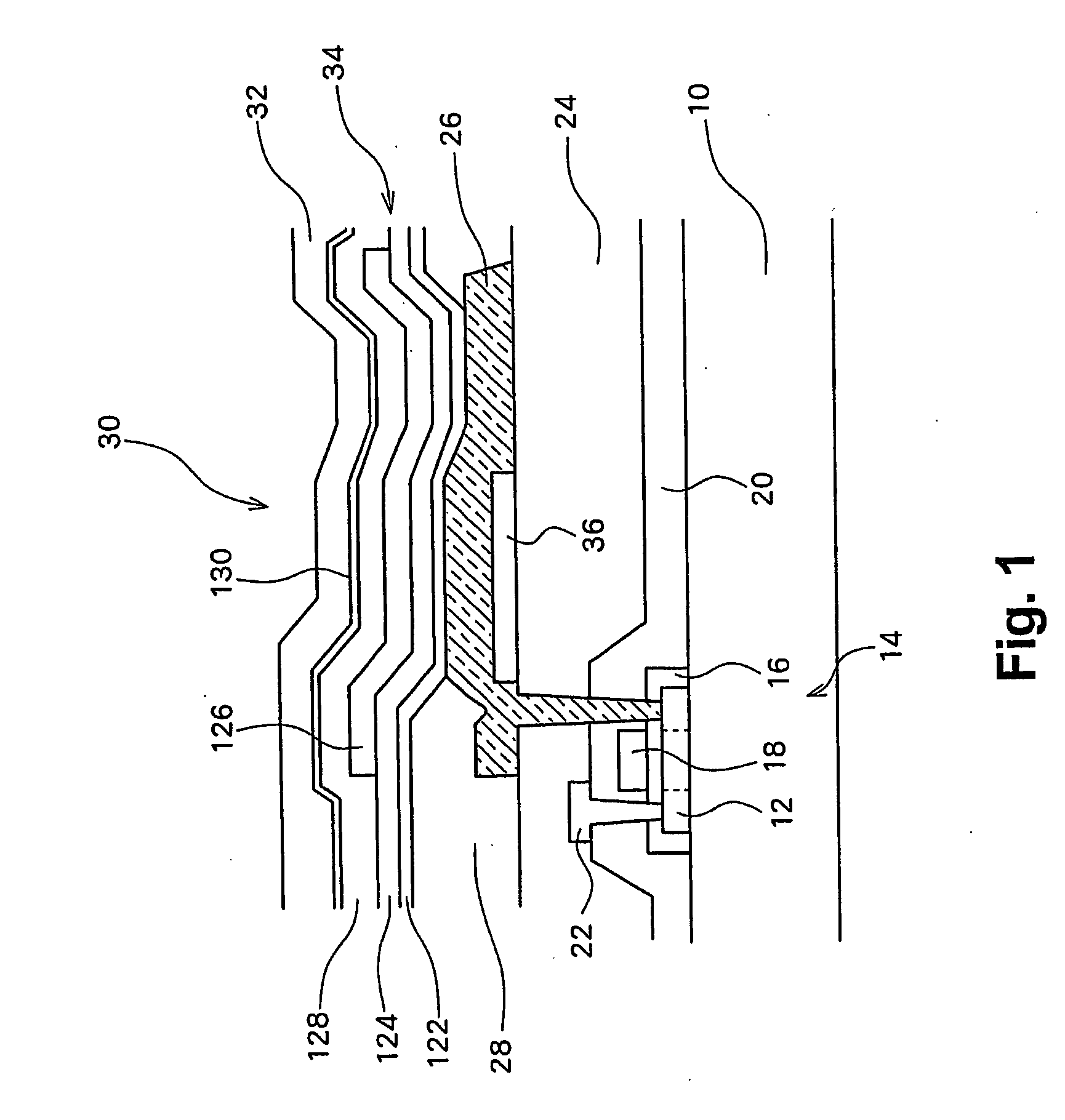
[0025]FIG. 1 is a cross-sectional view schematically showing the arrangement of a microcavity structure in a pixel of a display panel in accordance with a first embodiment of the present invention.

[0026] A semiconductor layer 12, formed at a predetermined place of a glass substrate 10, can constitute a TFT, electrodes, or wiring. According to the example shown in FIG. 1, the semiconductor layer 12 constitutes source, channel, and drain regions of a drive TFT 14. A gate insulating film 16 covers the semiconductor layer 12 of the drive TFT 14. A gate electrode 18, formed on the gate insulating film 16, is positioned above the channel region of the semiconductor layer 12.

[0027] An interlayer insulating film 20, formed on the gate electrode 18 and the gate insulating film 16, entirely covers the upper surface of the glass substrate 10. A source electrode 22, extending across the interlayer insulating film 20, contacts the source region of the drive TFT 14. A first flattening film 24 c...

second embodiment

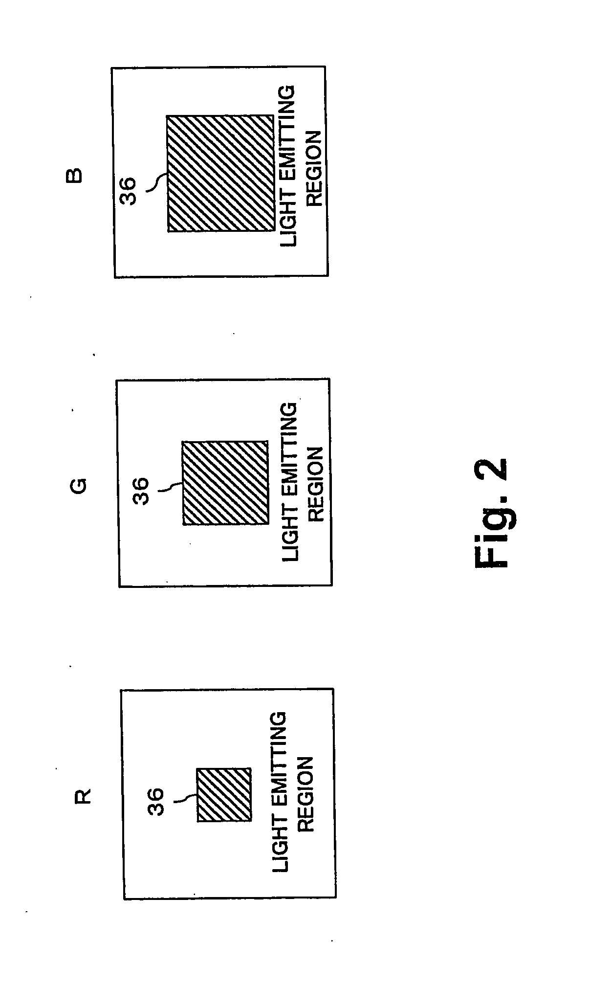
[0043]FIG. 3 shows an essential structure of a pixel in accordance with a second embodiment of the present invention. The lower reflection film 36 of the second embodiment covers the entire surface of the light emitting region. The organic layer 34 is partly thickened in a predetermined region of the light emitting region. According to the example of the second embodiment, the hole transporting layer 124 is relatively thick in a left part of the light emitting region and relatively thin in a right part of the light emitting region.

[0044] The characteristics of the microcavity structure can be determined according to the distance (i.e., cavity length) between the upper reflection film and the lower reflection film. Accordingly, in the present embodiment, the organic layer 34 having a partly changed thickness can provide two regions in the light emitting layer which are differentiated in cavity length. Thus, the wavelength of the light enhanced by the microcavity structure can be loc...

third embodiment

[0077]FIG. 7 shows an essential structure of a pixel in accordance with a third embodiment of the present invention. The lower reflection film 36 of the third embodiment covers the entire surface of the light emitting region. The lower reflection film 36 of the third embodiment is constituted by the above-described multilayered dielectric films. The thickness of the lower reflection film 36 is locally differentiated in each pixel (i.e., in one light emitting region).

[0078] More specifically, a thick region of the lower reflection film 36 can be constituted by a larger number of dielectric film layers while a thin region of the lower reflection film 36 can be constituted by a smaller number of dielectric film layers. According to the example shown in FIG. 7, the lower reflection film 36 is thick in a left part of the light emitting region and thin in a right part of the light emitting region.

[0079] The characteristics of the microcavity structure can be determined according to the ...


PUM


Abstract

Each pixel includes a region where a lower reflection film is not present. In each pixel, there is a region where a microcavity structure is formed between a counter electrode and a lower reflection film and another region where the microcavity structure is not formed. The regions differentiated in cavity length can differently enhance the peak wavelength so as to improve the viewing angle dependence. Furthermore, in each of R, G, and B light emitting pixels, the area ratio of a region where the microcavity structure is present and another region where the microcavity structure is not present can be adjusted so as to eliminate the differences caused by the microcavity structure.

Description

CROSS-REFERENCE TO RELATED APPLICATIONS [0001] The entire disclosure of Japanese Patent Application No. 2005-53894 filed Feb. 28, 2005 including specification, claims, drawings, and abstract is incorporated herein by reference. BACKGROUND OF THE INVENTION [0002] 1. Field of the Invention [0003] The present invention relates to an organic EL panel including plural pixels each having an organic EL element, and more particularly to an organic EL panel having, in each pixel, a micro-resonator (i.e., microcavity) capable of enhancing the light of a specific wavelength. [0004] 2. Description of the Related Art [0005] A flat panel display (FPD) is a prospective display device having a thin and compact structure. Some liquid crystal displays, which are a type of FPD, are practically used in various devices. Furthermore, there are light emitting devices (e.g., display devices or light sources) including self-luminous type electro-luminescence elements (hereinafter, referred to as “EL element...

Claims


Application Information

Patent Timeline
IPC IPC(8): H01L33/00G09F9/30H01L27/32H01L51/50H05B33/12H05B33/24H05B33/28
CPCH01L27/3211H01L27/3244H01L51/5265H01L2251/5323H10K59/35H10K59/12H10K50/852H10K2102/3031H10K2102/351H04M1/0237
Inventor NISHIKAWA, RYUJIOMURA, TETSUJINAKAI, MASAYA
Owner SANYO ELECTRIC CO LTD
Why Eureka
Try Eureka