Unlock instant, AI-driven research and patent intelligence for your innovation.

Method of surface processing substrate, method of cleaning substrate, and programs for implementing the methods

a surface processing and substrate technology, applied in the direction of cleaning with liquids, instruments, lighting and heating apparatus, etc., can solve the problems of reducing the properties of electronic devices manufactured from wafers, suppressing the formation of watermarks, and prone to becoming dirty on the wafer surface, so as to achieve the effect of cleaning the substra

Inactive Publication Date: 2006-09-07
TOKYO ELECTRON LTD
View PDF18 Cites 53 Cited by
  • Summary
  • Abstract
  • Description
  • Claims
  • Application Information

AI Technical Summary

Benefits of technology

[0017] According to the above method, the deposit on the substrate that has been cleaned with the liquid chemical is exposed to an atmosphere of a mixed gas containing ammonia and hydrogen fluoride under a predetermined pressure, and then the deposit that has been exposed to the atmosphere of the mixed gas is heated to a predetermined temperature. Upon the deposit being exposed to the atmosphere of the mixed gas containing ammonia and hydrogen fluoride under the predetermined pressure, a product that is a complex based on the deposit and the mixed gas is produced. Then, upon the product being heated to the predetermined temperature, the product is vaporized. Through the product being vaporized, the deposit, for example oxide, on the substrate can be removed. It is thus possible to remove the deposit, for example oxide, from the substrate so as to obtain a clean substrate.
[0049] According to the above method, the substrate having connecting holes fabricated in a first layer formed on the substrate by etching using a photoresist layer having a predetermined pattern formed on the first layer is subjected to removal of the photoresist layer, then to cleaning with SC1, then to cleaning with a hydrogen fluoride aqueous solution, then to cleaning with SC2, then to drying, then to exposure to an atmosphere of a mixed gas containing ammonia and hydrogen fluoride under a predetermined pressure, and then to heating to a predetermined temperature. As a result, contamination, native oxide and so on can be removed. Moreover, although watermarks are formed as deposit through the drying, effects as for the first aspect can be achieved, i.e. the deposit on the substrate can be removed. A clean substrate can thus be obtained. In particular, because cleaning with SC2 which can remove metal contamination is carried out, the present cleaning method is effective for cleaning a substrate having metal contamination attached thereto as deposit.

Problems solved by technology

Such watermarks act as masking in etching processing carried out after the cleaning processing, and hamper film formation processing, and hence may cause a degradation in properties of an electronic device manufactured from the wafer.
Suppressing the formation of watermarks in the cleaning processing is thus an issue in cleaning / drying art.
Meanwhile, in the spin drying step described above, the wafer is rotated at high speed and hence may become charged so that particles become electrostatically attached thereto, or may have dust or contaminating mist from the rotating apparatus attached thereto.
There is thus a problem that the wafer surface is prone to becoming dirty.
Moreover, native oxide of film thickness not less than 0.5 nm is formed on a wafer surface exposed to the atmosphere, and it is known that such native oxide is a large problem for forming a gate insulating film of film thickness not more than 65 nm.
Even though formation of watermarks is suppressed by using IPA drying, it has thus been difficult to obtain a clean wafer surface after the drying.

Method used


Image

  • Method of surface processing substrate, method of cleaning substrate, and programs for implementing the methods
  • Method of surface processing substrate, method of cleaning substrate, and programs for implementing the methods
  • Method of surface processing substrate, method of cleaning substrate, and programs for implementing the methods

Examples


Embodiment Construction

[0077] The present invention will now be described in detail with reference to the drawings showing preferred embodiments thereof.

[0078] First, a method of surface processing a substrate according to an embodiment of the present invention will be described.

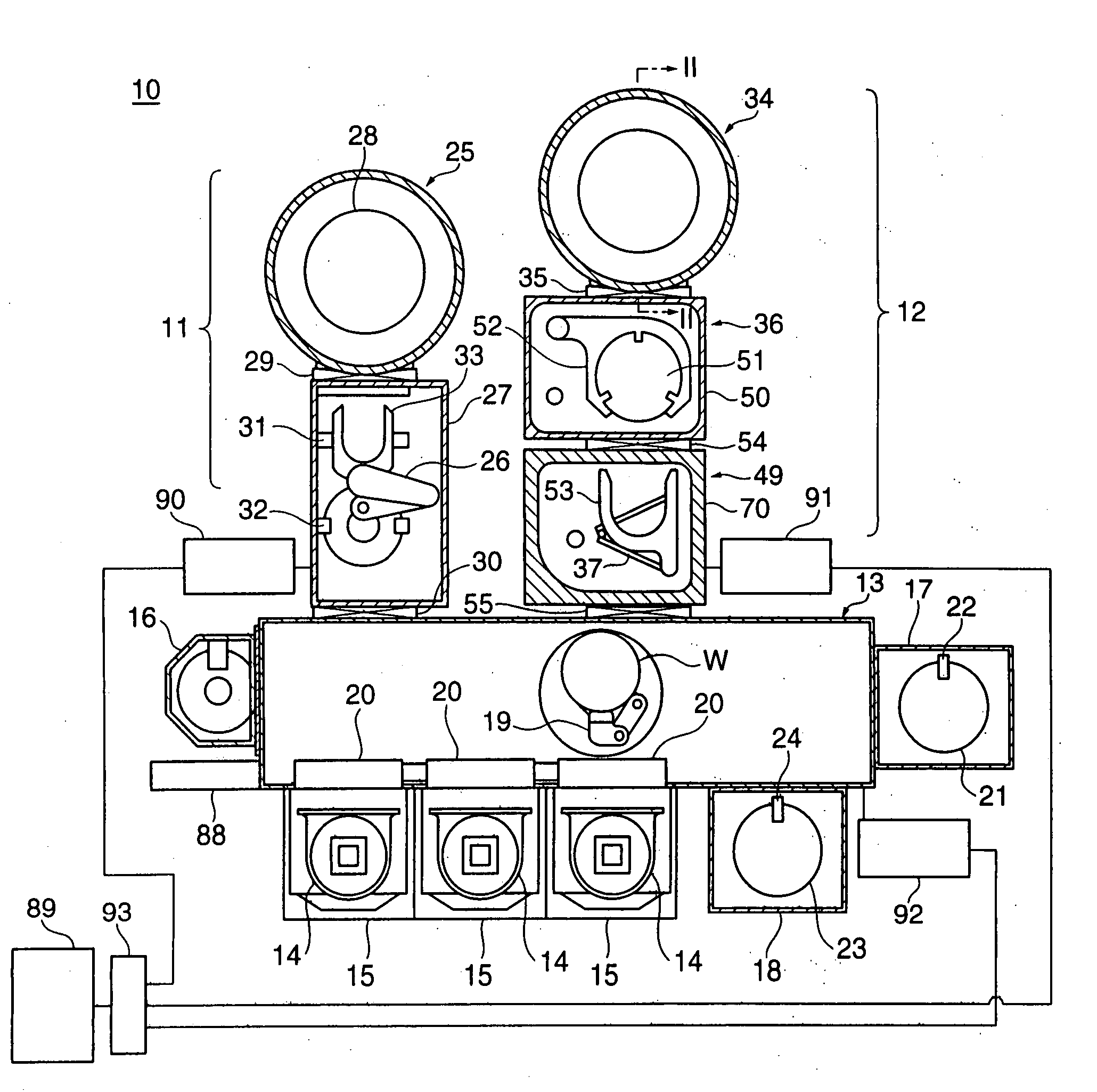
[0079]FIG. 1 is a plan view schematically showing the construction of a substrate processing apparatus to which is applied the method of surface processing a substrate according to the present embodiment.

[0080] As described below, the substrate processing apparatus implements COR cleaning processing as post-processing in cleaning processing for removing contamination attached to a surface, or native oxide formed on the surface, of an electronic device wafer in which contact holes or the like have been formed.

[0081] As shown in FIG. 1, the substrate processing apparatus 10 is comprised of a first process ship 11 for carrying out reactive ion etching (hereinafter referred to as “RIE”) processing on electronic device wafers (here...


PUM

PropertyMeasurementUnit
Temperatureaaaaaaaaaa
Pressureaaaaaaaaaa
Temperatureaaaaaaaaaa

Abstract

A method of surface processing a substrate that enables deposit to be removed from a substrate so as to obtain a clean substrate. A substrate is cleaned with a liquid chemical. A deposit which is formed through the cleaning with liquid chemical is exposed to an atmosphere of a mixed gas containing ammonia and hydrogen fluoride under a predetermined pressure. The deposit that has been exposed to the atmosphere of the mixed gas is heated to a predetermined temperature.

Description

BACKGROUND OF THE INVENTION [0001] 1. Field of the Invention [0002] The present invention relates to a method of surface processing a substrate, a method of cleaning a substrate, and programs for implementing the methods, and more particularly to a method of surface processing a substrate in which silicon oxide (SiO2) that has been formed on a substrate surface is removed. [0003] 2. Description of the Related Art [0004] Conventionally, a wet cleaning method has been widely used for removing particles, contamination such as a surface coating film of adsorbed molecules, metal or organic matter, and silicon native oxide on a silicon wafer (hereinafter referred to merely as a “wafer”), and for removing watermarks or the like formed on a wafer. The art that forms the basis of the conventional wet cleaning method is the RCA cleaning method, which was developed in the 1960's, and many cleaning methods using this art have been proposed. [0005] Of wafer surface cleaning methods, for example ...

Claims


Application Information

Patent Timeline
IPC IPC(8): C23G1/00B08B7/00B08B3/00C23F1/00C03C15/00B44C1/22
CPCG03F7/423G03F7/425H01L21/02049H01L21/02063H01L21/02068H01L21/67028H01L21/67161H01L21/67167H01L21/67184H01L21/6719
Inventor NISHIMURA, EIICHIORII, TAKEHIKO
Owner TOKYO ELECTRON LTD