Method of manufacturing thin film transistor, thin film transistor manufactured by the method, and display device employing the same

Active Publication Date: 2006-09-07
SAMSUNG DISPLAY CO LTD
View PDF2 Cites 18 Cited by
  • Summary
  • Abstract
  • Description
  • Claims
  • Application Information

AI Technical Summary

Benefits of technology

[0015] The present invention has been made to overcome the above and other problems, and it is an object of the present invention to provide a metho

Problems solved by technology

The organic semiconductor material such as pentacene and polythiophene is difficult and complicated to be patterned since it has poor chemical and optical stability.
In addition, even after being patte

Method used


Image

  • Method of manufacturing thin film transistor, thin film transistor manufactured by the method, and display device employing the same
  • Method of manufacturing thin film transistor, thin film transistor manufactured by the method, and display device employing the same
  • Method of manufacturing thin film transistor, thin film transistor manufactured by the method, and display device employing the same

Examples


Example

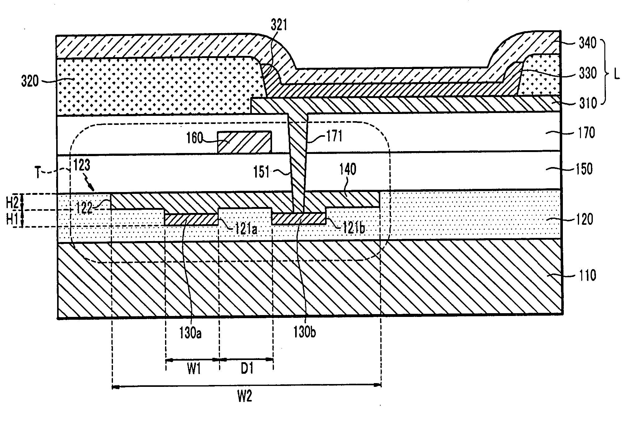
[0038] First, a method of manufacturing a TFT according to the first embodiment of the present invention will be described with reference to FIGS. 1A to 1F and FIG. 2.

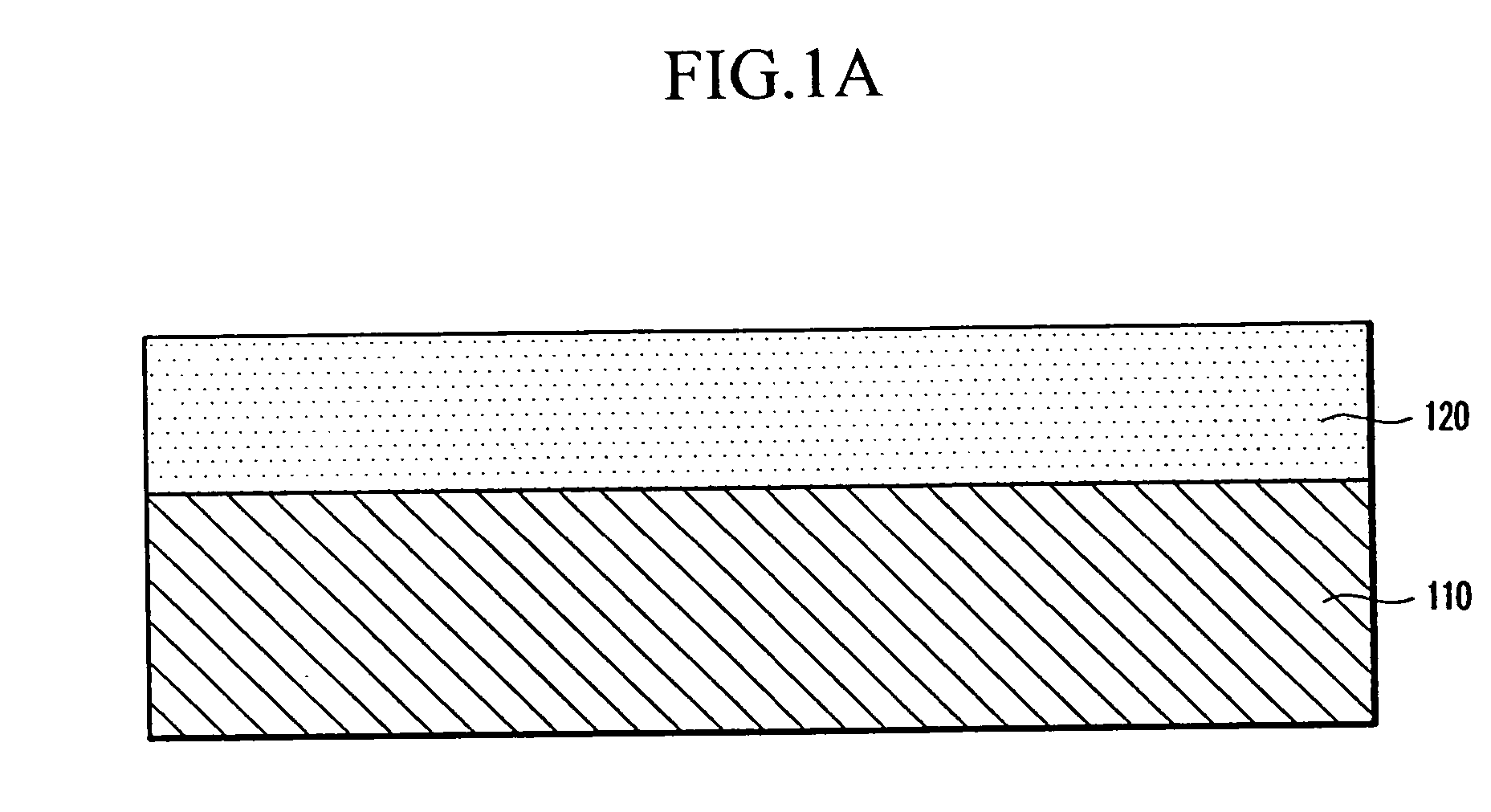
[0039] Referring to FIG. 1A, an organic insulating film 120 is coated on a substrate 110. The substrate 110 can be made of insulating material such as glass or plastic or metal material such as stainless steel (SUS). The plastic can be polyethylene terephthalate (PET), polyethylene naphthalate (PEN), polyether sulfone (PES), polyether imide, polyphenylene sulfide (PPS), polyarylate(PAR), polyimide, polycarbonate (PC), polyacrylate, cellulose triacetate and cellulose acetate propionate (CAP), etc. The organic insulating film 120 can be made of negative type photoresist.

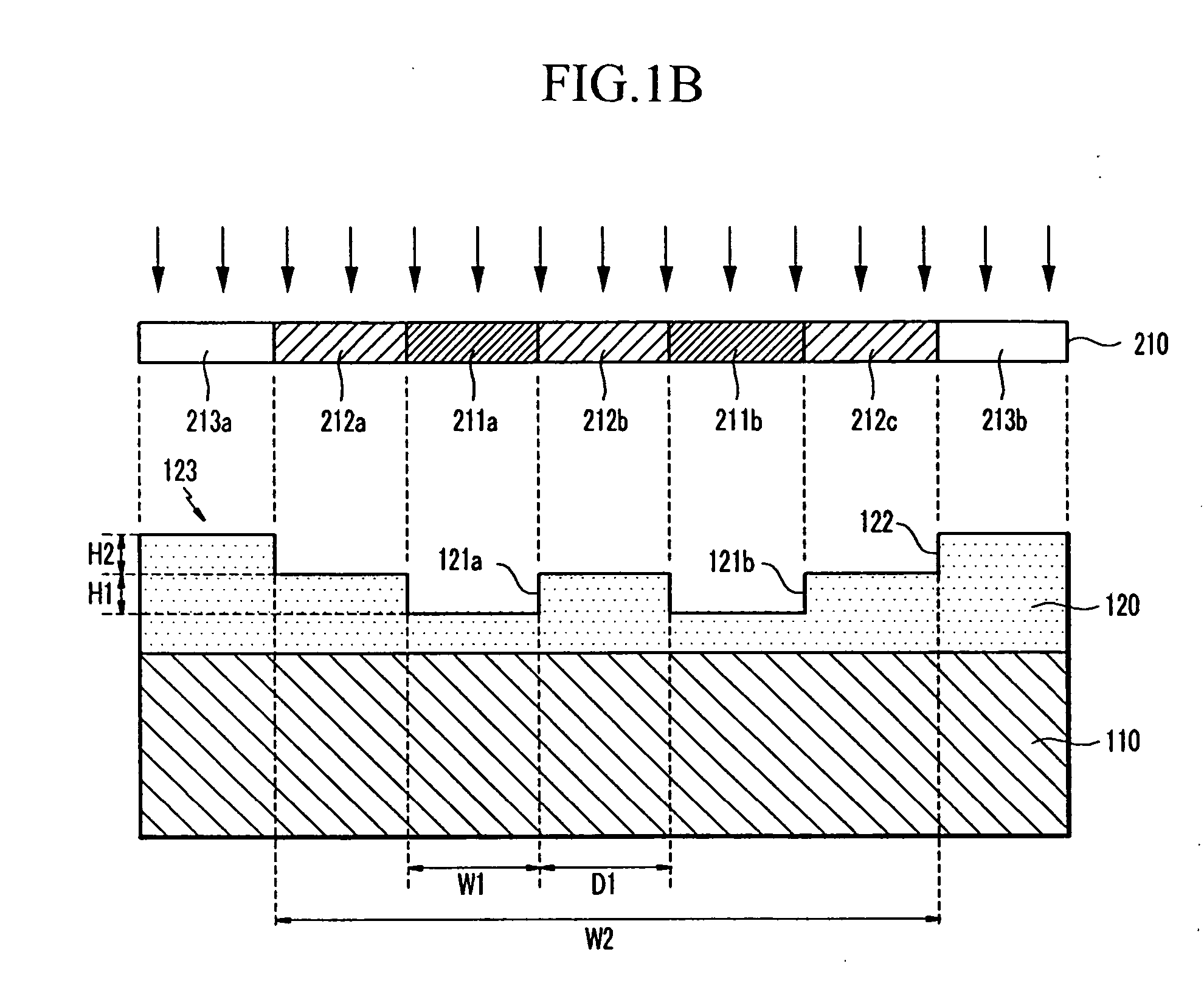
[0040] Referring to FIG. 1B, the organic insulating film 120 is exposed using a half tone mask 210 and the exposed organic insulating film 120 is developed, to form a bank 123 having first, second and third concave portions 121a, 121b and 122 in the org...


PUM

PropertyMeasurementUnit
Widthaaaaaaaaaa
Widthaaaaaaaaaa
Widthaaaaaaaaaa

Abstract

A method of manufacturing a thin film transistor is capable of enhancing pattern precision of an organic semiconductor layer and simplifying a patterning process. The method includes forming an organic insulating film on a substrate and forming a bank having the first and second concave portions and a third concave portion in the organic insulating film, the third concave portion being formed on the first and second concave portions. The method further includes forming a source electrode and a drain electrode in the first and second concave portions and forming an active layer in the third concave portion, the active layer contacting the source electrode and the drain electrode.

Description

CLAIM OF PRIORITY [0001] This application makes reference to, incorporates the same herein, and claims all benefits accruing under 35 U.S.C. §119 from applications earlier filed in the Korean Intellectual Property Office on 4 Mar. 2005 and 8 Feb. 2006 and there duly assigned Serial Nos. 10-2005-0018164 and 10-2006-0012088, respectively. BACKGROUND OF THE INVENTION [0002] 1. Field of the Invention [0003] The present invention relates to a thin film transistor, and more particularly to a method of manufacturing a thin film transistor using an organic semiconductor material as an active layer, a thin film transistor manufactured by the method, and a display device employing the same. [0004] 2. Description of the Related Art [0005] A display device such as an organic light emitting display and a liquid crystal display which are small in thickness and operate with low voltages, unlike a cathode ray tube (CRT) which is bulky and operates with high voltages, is being widely used as the nex...

Claims


Application Information

Patent Timeline
IPC IPC(8): H01L29/08
CPCH01L27/3244H01L51/0021H01L51/0036H01L51/0037H01L51/0038H01L51/0052H01L51/0053H01L51/0097H01L51/0516H01L51/0545H01L51/105H10K59/12H10K71/60H10K85/113H10K85/1135H10K85/114H10K85/621H10K85/615H10K77/111H10K10/468H10K10/466H10K10/84
Inventor SUH, MIN-CHULKOO, JAE-BON
Owner SAMSUNG DISPLAY CO LTD
Why Eureka
Try Eureka