Shift register circuit and drive control apparatus

a technology of shift register and control apparatus, which is applied in the direction of digital storage, instruments, vehicle components, etc., can solve the problems of disadvantageously difficult to apply to a panel having a large number of scanning lines, high operating frequency, and low electron mobility, so as to suppress the deterioration of characteristics during operation and reduce the effect of electron mobility

Active Publication Date: 2006-09-21
ORTUS TECH
View PDF5 Cites 79 Cited by
  • Summary
  • Abstract
  • Description
  • Claims
  • Application Information

AI Technical Summary

Benefits of technology

[0020] The present invention has, in a shift register circuit which sequentially transfers an input signal and sequentially outputs an output signal and a drive control apparatus including this shift register circuit, an advantage that deterioration in characteristics during an operation can be suppressed and an output signal can be excellently output at a predetermined timing over a relatively long period even if a switching element having element characteristics that electron mobility is relatively low is applied in the shift register circuit.

Problems solved by technology

As described above, in the thin film transistor element formed of a semiconductor material such as amorphous silicon or zinc oxide, its electron mobility is low and its operation characteristics are poor as compared with a thin film transistor element formed of a semiconductor material such as single-crystal silicon or polysilicon.
However, in the scanning driver to which an amorphous silicon transistor or the like is applied, since its operating frequency is essentially low, it is disadvantageously hard to be applied to a panel having a large number of scanning lines and a high operating frequency, e.g., a display panel having a high resolution or a large screen or a sensor array.
Therefore, considerably reducing the operating frequency to be lower than that of the scanning driver to which a single-crystal silicon transistor is applied is unavoidable.
Therefore, it has a problem that excellently performing display driving or read driving for a long time is difficult.
Specifically, according to a verification by the present inventors, there has been obtained an experimental result that an operating frequency is reduced to approximately ½ of that in the initial state when an acceleration experiment is conducted for several-hundred hours in a temperature environment of approximately 80° C. There is a problem that excellent display driving or read driving cannot be assured in an actual product for a long period of time.

Method used


Image

  • Shift register circuit and drive control apparatus
  • Shift register circuit and drive control apparatus
  • Shift register circuit and drive control apparatus

Examples


first application example

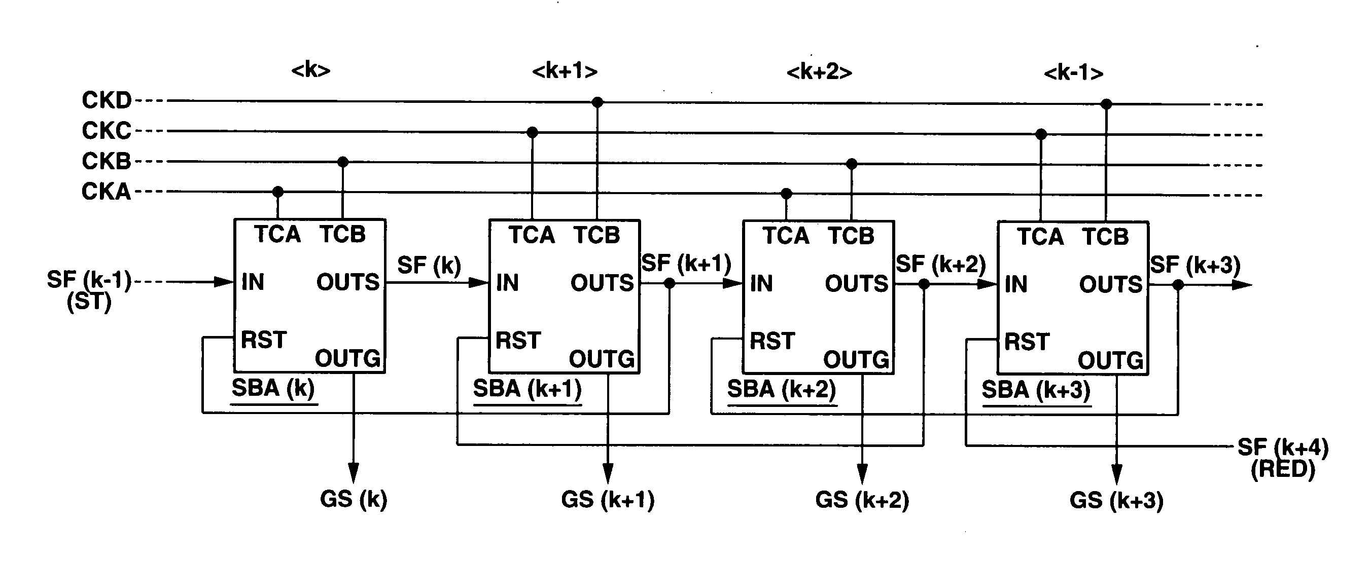
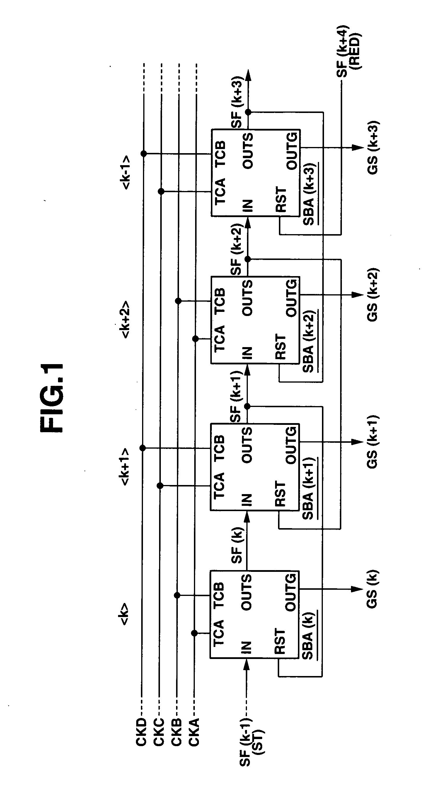
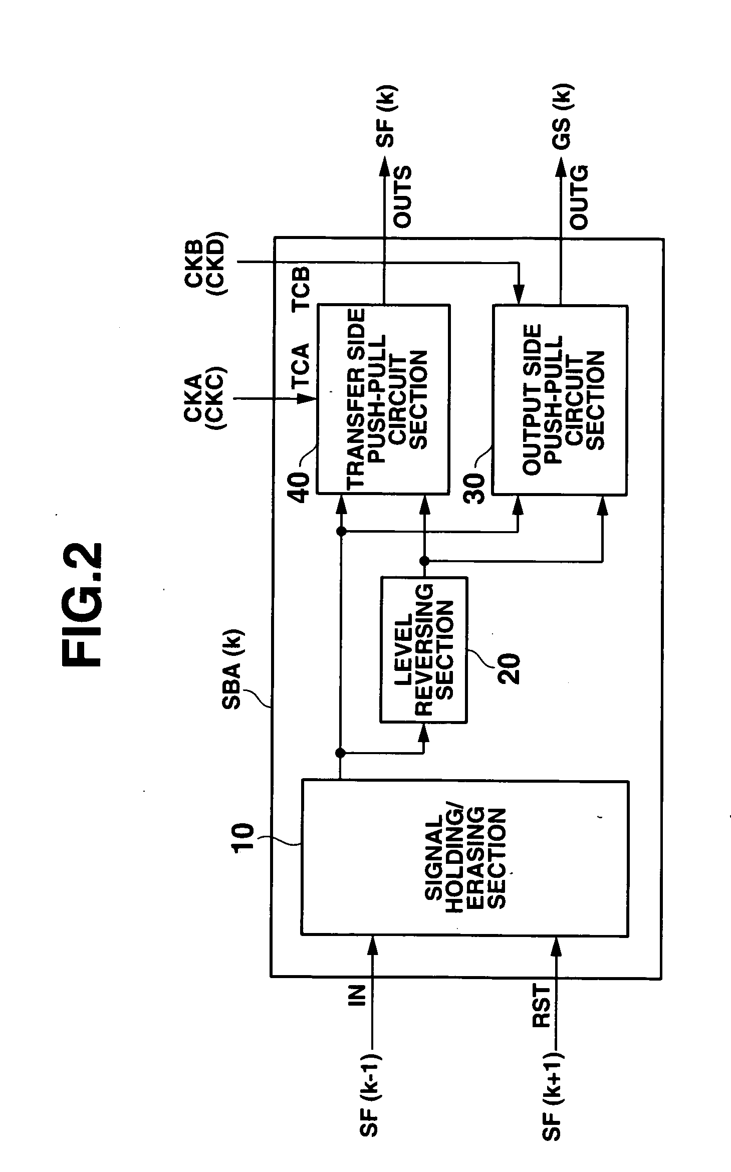
[0109]FIG. 5 is a schematic structural view showing an entire structure of an image display apparatus in which the shift register circuit according to the present invention is applied to a scanning driver (a drive control apparatus).

[0110]FIGS. 6A and 6B are schematic circuit diagrams showing structural examples of a display pixel constituting a display panel in the image display apparatus according to the first application example.

[0111] As shown in FIG. 5, an image display apparatus 100 according to this application example is roughly configured to include: a display panel (a display pixel array) 110 which has a plurality of display pixels EM two-dimensionally arranged therein and corresponds to an active matrix drive mode; an odd-numbered line scanning driver (a first drive control section) 120L which is connected with odd-numbered scanning lines (which will be referred to as “odd-numbered side lines” hereinafter for the convenience's sake) SLo alone of scanning lines which ext...

second application example

[0161] A second application example of a shift register circuit according to this embodiment will now be described with reference to the accompanying drawings.

[0162]FIG. 10 is a schematic structural view showing an example of a shift register circuit of an odd-numbered line scanning driver in an image display apparatus according to the second application example.

[0163]FIG. 11 is a schematic structural view showing an example of a shift register circuit of an even-numbered line scanning driver in the image display apparatus according to the second application example.

[0164] Here, like or corresponding reference numerals denote structures equivalent to those in the first application example, thereby eliminating their explanation. It is to be noted that the entire configuration of the image display apparatus according to this application example is equivalent to the first application example (see FIG. 5), thus eliminating its explanation.

[0165] First, in this application example, e...


PUM


Abstract

A shift register circuit includes a plurality of cascade-connected signal holding circuits each of the signal holding circuits includes an input control circuit to which an input signal is applied, and which fetches and holds the input signal, an output control circuit to which a first control clock signal is applied, and which outputs an output signal corresponding to timings of the held input signal and the first control clock signal, and a reset control circuit to which a reset signal is applied, and which initializes a signal level of the input signal held in the input control circuit. A timing at which the output signal is terminated is set to be ahead of an application start timing of the reset signal.

Description

CROSS-REFERENCE TO RELATED APPLICATIONS [0001] This application is based upon and claims the benefit of priority from prior Japanese Patent Application No. 2005-072710, filed Mar. 15, 2005, the entire contents of which are incorporated herein by reference. BACKGROUND OF THE INVENTION [0002] 1. Field of the Invention [0003] The present invention relates to a shift register circuit and a drive control apparatus, and more particularly to a shifter register circuit which can be excellently applied in a scanning driver of, e.g., an image display apparatus or an image read apparatus, and a drive control apparatus including this shift register circuit. [0004] 2. Description of the Related Art [0005] In recent years, information devices such as a computer, a mobile phone or a personal digital assistance, or imaging devices such as a digital video camera, a digital still camera or a scanner have considerably gained in popularity. In such devices, an image display circuit for, e.g., a liquid ...

Claims


Application Information

Patent Timeline
Patent Type & Authority Applications(United States)
IPC IPC(8): G11C19/00
CPCG11C19/00G11C19/28B60R7/10B60R7/043B60R2011/0017
Inventor YAMAGUCHI, IKUHIROMOROSAWA, KATSUHIKO
Owner ORTUS TECH
Why Eureka
Try Eureka