Carbon nanotube device and manufacturing method of the same

a carbon nanotube and manufacturing method technology, applied in the direction of carbonsing rags, fibre chemical treatment, fibre treatment, etc., can solve the problems of inability to connect between two spots apart from each other horizontally by carbon nanotubes, and the shape limitation of carbon nanotubes formed according to these methods

Inactive Publication Date: 2006-09-21
FUJITSU LTD
View PDF3 Cites 20 Cited by
  • Summary
  • Abstract
  • Description
  • Claims
  • Application Information

AI Technical Summary

Benefits of technology

[0012] In a manufacturing method of the carbon nanotube according to the present invention, after a catalytic layer and a body extending to a position above the catalytic lay...

Problems solved by technology

However, there is a limitation in shape of the carbon nanotube formed according to these methods only.
Furthermore, under a circumstance wher...

Method used


Image

  • Carbon nanotube device and manufacturing method of the same
  • Carbon nanotube device and manufacturing method of the same
  • Carbon nanotube device and manufacturing method of the same

Examples


first embodiment

[0034] First Embodiment

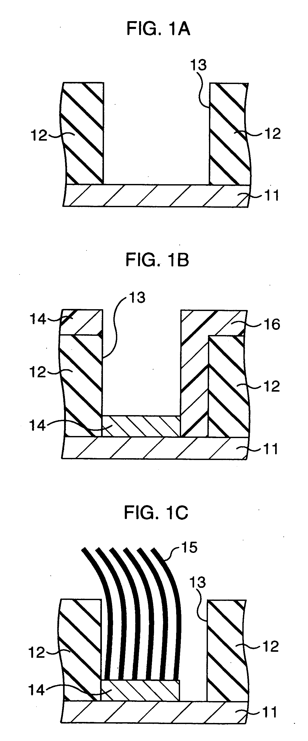
[0035] Firstly, a first embodiment of the present invention will be explained. FIG. 1A to FIG. 1C are sectional views showing a manufacturing method of a carbon nanotube device according to the first embodiment of the present invention in process order.

[0036] In the first embodiment, as shown in FIG. 1A, a SiO2 film 12 is first formed on a silicon (Si) substrate 11. The SiO2 film 12 is, for instance, about 350 nm in thickness. Next, a cylindrical opening 13 is formed in the SiO2 film 12 by patterning with a resist pattern (not shown). The opening 13 is, for instance, about 2 μm in diameter.

[0037] Then, a resist film is formed on the entire surface, and a resist pattern 16 is formed by patterning the resist film, as shown in FIG. 1B. The resist pattern 16 has a shape covering the bottom of the opening 13 on only one side. As a result, the Si substrate 11 is exposed only from a part of the opening 13. In the present embodiment, especially when the resist patte...

second embodiment

[0043] Second Embodiment

[0044] Next, a second embodiment of the present invention will be explained next. FIG. 4A to FIG. 4C are sectional views showing a manufacturing method of a carbon nanotube device according to the second embodiment of the present invention in process order.

[0045] First, in the second embodiment, as shown in FIG. 4A, a catalytic layer 24 is selectively formed on a Si substrate 21. As the catalytic layer 24, for instance, a cobalt (Co) film having a thickness of about 1 nm is formed.

[0046] Next, a SiO2 film 22 is formed over the entire surface thereof. Then, a groove 23 is formed in the SiO2 film 22 by patterning using a resist pattern (not shown). The thickness of the SiO2 film 22 is, for instance, about 350 nm. When forming the groove 23, as shown in FIG. 4B, both of the Si substrate 21 and the catalytic layer 24 are to be exposed from the groove 23.

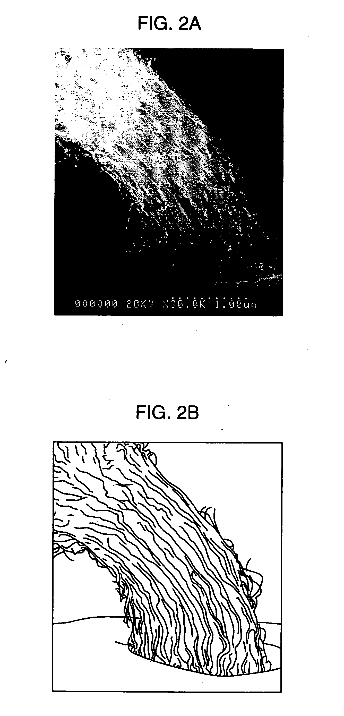
[0047] Thereafter, as shown in FIG. 4C, carbon nanotubes 25 are grown on the catalytic layer 24. At this tim...

third embodiment

[0050] Third Embodiment

[0051] Next, a third embodiment of the present invention will be explained next. FIG. 7A to FIG. 7B are sectional views showing a manufacturing method of a carbon nanotube device according to the third embodiment of the present invention in process order.

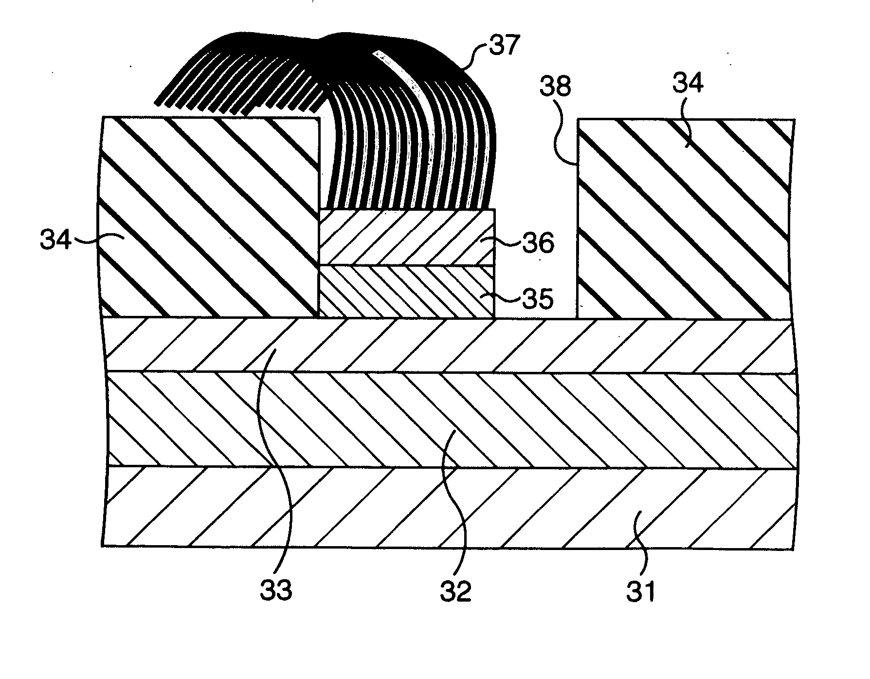
[0052] In the third embodiment, first, as shown in FIG. 7A, a copper (Cu) film 32 and a tantalum (Ta) film 33 are formed in sequence on a Si substrate 31 by, for instance, a sputtering method. The Cu film 32 and the Ta film 33 are about 150 nm and about 5 nm in thickness, respectively. Then, a SiO2 film 34 is formed over the entire surface. The SiO2 film 34 is, for instance, about 350 nm in thickness. Next, a cylindrical opening 38 is formed on the SiO2 film 34 by patterning with a resist pattern (not shown). The opening 38 is, for instance, about 2 μm in diameter.

[0053] Then, similarly to the first embodiment, a resist film is formed on the entire surface, and a resist pattern (not shown) is formed by patte...


PUM


Abstract

After forming an opening, a resist film is formed on the entire surface and a resist pattern is formed by patterning the resist film. The shape of the resist pattern is such that it covers one side of the bottom of the opening. As a result, a Si substrate is exposed only in one part of the opening. Then, using the resist pattern as a mask, a catalytic layer is formed on the bottom of the opening. Then, the resist pattern is removed. Carbon nanotubes are grown on the catalytic layer. At this time, since the catalytic layer is formed on only one side of the bottom of the opening, the Van der Waals force biased towards that side works horizontally on the growing carbon nanotubes. Therefore, the carbon nanotubes are attracted towards the nearest side of the SiO2 film and grow biased towards that side.

Description

CROSS-REFERENCE TO RELATED APPLICATIONS [0001] This application is based upon and claims the benefit of priority from the prior Japanese Patent Application No. 2005-080519, filed on Mar. 18, 2005, the entire contents of which are incorporated herein by reference.BACKGROUND OF THE INVENTION [0002] 1. Field of the Invention [0003] The present invention relates to a carbon nanotube device suitable for integrated circuits and the like and a manufacturing method of the same. [0004] 2. Description of the Related Art [0005] In recent years, many researches have been directed to application of a carbon nanotube to semiconductor devices. As a method of obtaining a carbon nanotube, a catalytic layer is arranged in a hole formed in an insulating film, and the carbon nanotubes are grown vertically from the catalytic layer as shown in FIG. 11A, FIG. 11B, FIG. 12A and FIG. 12B. [0006] In addition to the above method, there is a method of growing a carbon nanotube in a horizontal direction. This m...

Claims


Application Information

Patent Timeline
IPC IPC(8): D01F9/12D01C5/00
CPCB82Y30/00D01F9/12H01L21/76838H01L21/76876H01L21/76879H01L2221/1094
Inventor KAWABATA, AKIONIHEI, MIZUHISAKONDO, DAIYUSATO, SHINTARO
Owner FUJITSU LTD
Why Eureka
Try Eureka