Thin film photovoltaic device

a photovoltaic device and thin film technology, applied in the direction of thermoelectric devices, electrical devices with dielectric constant thermal change, semiconductor devices, etc., can solve the problems of increasing the overall volume of the photovoltaic device, increasing the complexity of the device fabrication, and only producing a couple of volts of photovoltaic voltag

Active Publication Date: 2006-09-28
AGENCY FOR SCI TECH & RES
View PDF6 Cites 25 Cited by
  • Summary
  • Abstract
  • Description
  • Claims
  • Application Information

AI Technical Summary

Benefits of technology

[0009] The term “thin film” or “thin film layer” is referred to in the context to define the characteristics of the light-electricity conversion component of the photovoltaic device, to distinguish from the bulk material such as bulk ferroelectric ceramic used in conventional devices. According to embodiments of the present invention, the thickness of the thin film layer is below about 10 micrometers. Most typically, the thickness of the thin film layer is below about 5 micrometers.

Problems solved by technology

Photovoltaic devices of the above kind, however, may only produce a photovoltaic voltage below a couple of volts, due to the fundamental limitation of the semiconductor photovoltaic effect.
The consequence of increasing the thickness of the ferroelectric layer is that, the fabrication of the device becomes more complicated and at higher cost.
The overall volume of the photovoltaic device also increases, which are not desirable characteristics in micro systems or micro devices, such as MEMS.
As such, ferroelectric thin film photovoltaic devices, much like the semiconductor photovoltaic device, are limited to producing a photovoltage of below one volt.
In many applications, particularly involving mechanical movement, such as MEMS, this low-level of voltage may be insufficient.

Method used


Image

  • Thin film photovoltaic device
  • Thin film photovoltaic device
  • Thin film photovoltaic device

Examples


Embodiment Construction

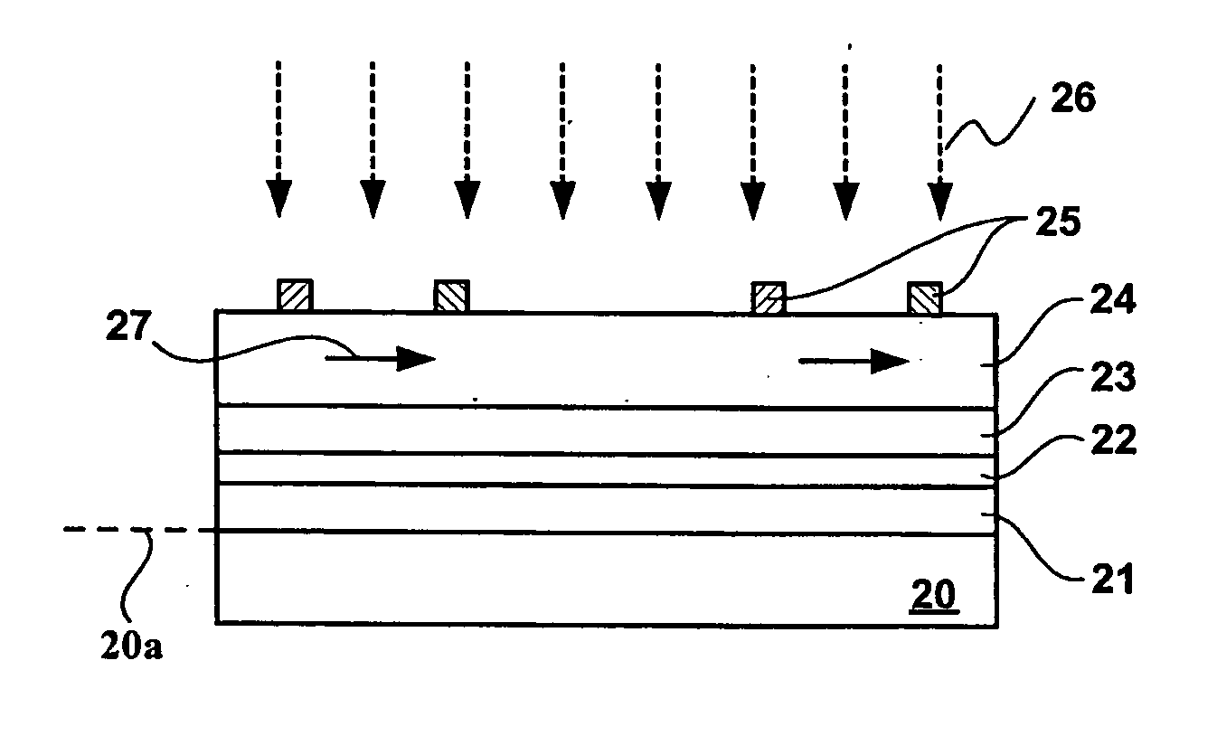
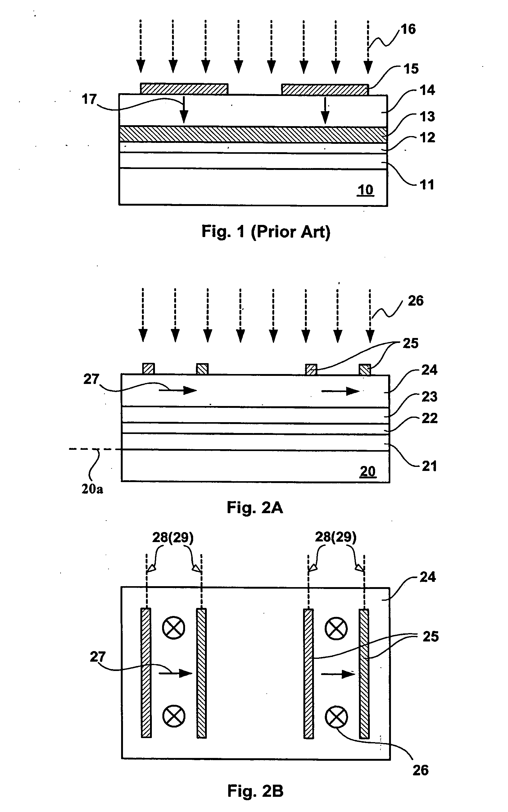
[0031] As shown in FIGS. 2A and 2B, a thin film photovoltaic device according to one embodiment of the present invention has a thin film layer, for example a ferroelectric thin film layer 24 formed on a substrate 20. Intermediate layers 21, 22 and 23 may be formed on substrate 20 prior to the formation of ferroelectric thin film layer 24. Intermediate layers 21, 22 and 23 are not all electrically conductive. One or more pairs of electrodes 25 are situated on the top surface of ferroelectric thin film layer 24. One of each pair of electrodes 25 is situated apart from another on the top surface of the ferroelectric thin film layer 24. An electric field 28 is applied between each pair of electrodes 25, to polarize the ferroelectric thin film layer 24. The ferroelectric polarization 27 is therefore aligned in the direction parallel to a main surface plane 20a of substrate 20, and hence parallel to the ferroelectric layer 24. According to this embodiment, when a beam of ultraviolet (UV) ...


PUM


Abstract

The present invention provides a thin film photovoltaic device and a method of forming a thin film photovoltaic device. The thin film photovoltaic device has a substrate, a thin film layer formed on the substrate and first and second electrodes formed on one side of the thin film layer. By applying an electric field over the first and second electrodes, the thin film layer is polarized in a direction parallel to the surface plane of the film. Upon exposure to light, the thin film layer converts light energy into electricity. According to the method, a thin film layer is formed on a substrate. A first electrode and a second electrode are formed on one side of the thin film layer. By applying an electric field over the first and second electrodes, the thin film layer is polarized in a direction parallel to the surface plane of the film.

Description

[0001] This application claims benefit of U.S. Provisional Patent Application No. 60 / 664,652 filed on Mar. 22, 2005, entitled “Photovoltaic Device”, which is hereby incorporated by reference.FIELD OF THE INVENTION [0002] The present invention relates to a photovoltaic device and in particular, to a thin film photovoltaic device made of ferroelectric material. BACKGROUND OF THE INVENTION [0003] Photovoltaic devices are used in several industrial applications to produce electricity under illumination of light. A conventional photovoltaic device has a semiconductor p-n junction and a pair of electrodes. Upon exposure to light, the semiconductor p-n junction converts the optical energy into electrical energy output via the electrodes. [0004] Photovoltaic devices of the above kind, however, may only produce a photovoltaic voltage below a couple of volts, due to the fundamental limitation of the semiconductor photovoltaic effect. To obtain a higher photovoltage, ferroelectric materials wi...

Claims


Application Information

Patent Timeline
Patent Type & Authority Applications(United States)
IPC IPC(8): H01L31/00
CPCH01L31/0264H02S99/00H01L37/02Y02E10/50H10N15/10
Inventor YAO, KUISHANNIGRAHI, SANTIRANJANCHEN, MEI M.GAN, BEE K.
Owner AGENCY FOR SCI TECH & RES
Why Eureka
Try Eureka