Fast-disabled voltage regulator circuit with low-noise feedback loop and operating method thereof
- Summary
- Abstract
- Description
- Claims
- Application Information
AI Technical Summary
Benefits of technology
Problems solved by technology
Method used
Image
Examples
Embodiment Construction
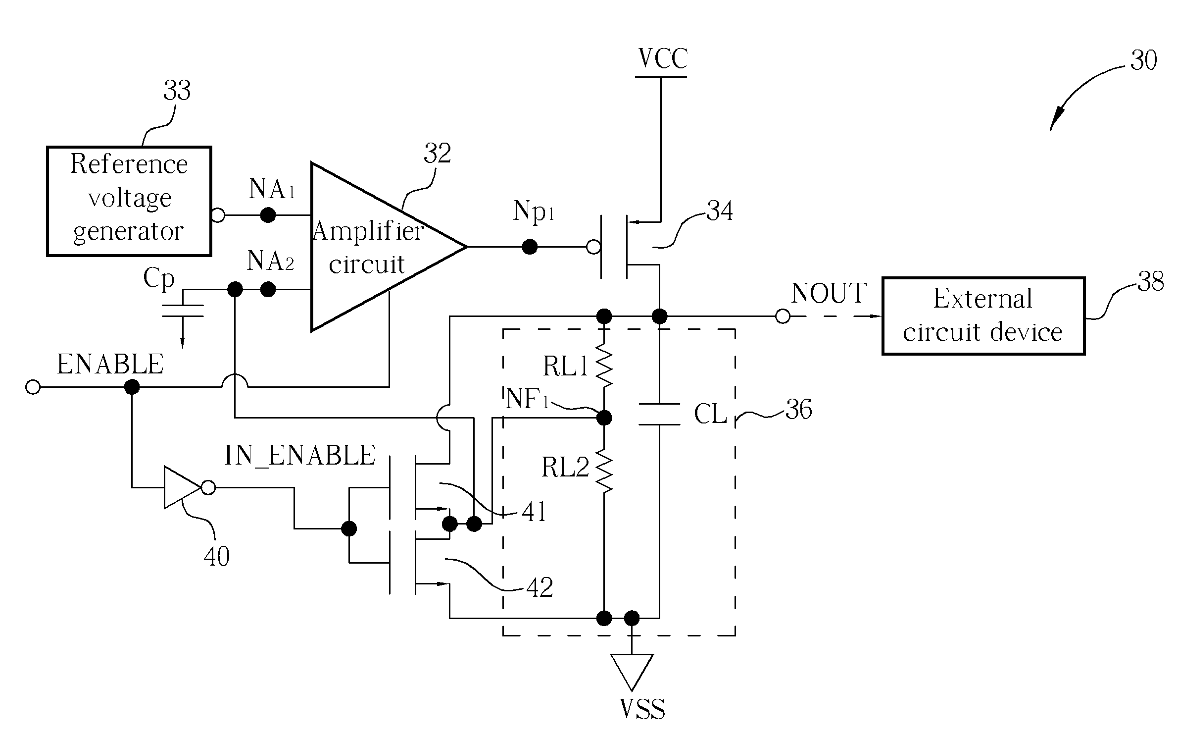
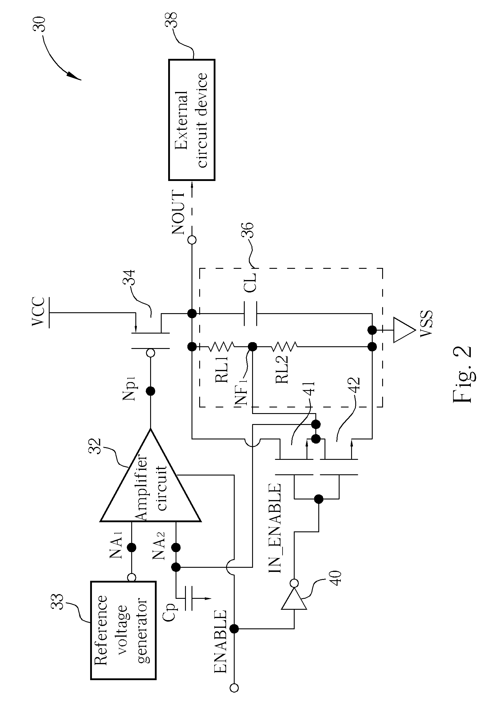
[0019] Technical characteristics of the present invention emphasizes on the operation when a low-noise voltage regulator circuit is disabled. Please refer to FIG. 2. FIG. 2 is a diagram of an embodiment of a low-noise voltage regulator circuit 30 according to the present invention. Please note that the voltage regulator circuit 30 shown in FIG. 2 is built by several MOS transistors and related circuit components. In practical implementation, other transistors, such as BJTs, can also be used to replace MOS transistors. Please refer to FIG. 2, the voltage regulator circuit 30 comprises an amplifier circuit 32, an output transistor 34, an inverter 40, a first discharge transistor 41, a second discharge transistor 42, and a loading module 36. In practical implementation, the amplifier circuit 32 can be an operational amplifier or a differential amplifier. The amplifier circuit 32 comprises an output terminal Np1, a first receiving terminal NA1, and a second receiving terminal NA2. The f...
PUM
 Abstract
Description
Claims
Application Information


