Controllable varactor within dummy substrate pattern

Inactive Publication Date: 2006-10-05
TAIWAN SEMICON MFG CO LTD
View PDF4 Cites 8 Cited by
  • Summary
  • Abstract
  • Description
  • Claims
  • Application Information

AI Technical Summary

Benefits of technology

[0006] It is therefore an object of the invention to provide an improved method to form dummy patterns to avoid active device performance degradation, while overcoming other deficiencies and shortcomings of the prior art.

Problems solved by technology

However, a problem in the prior art is that the formation of dummy patterns has been found to undesirably affect the electrical performance of devices formed in the active areas by parasitic coupling phenomena.

Method used


Image

  • Controllable varactor within dummy substrate pattern
  • Controllable varactor within dummy substrate pattern
  • Controllable varactor within dummy substrate pattern

Examples


Embodiment Construction

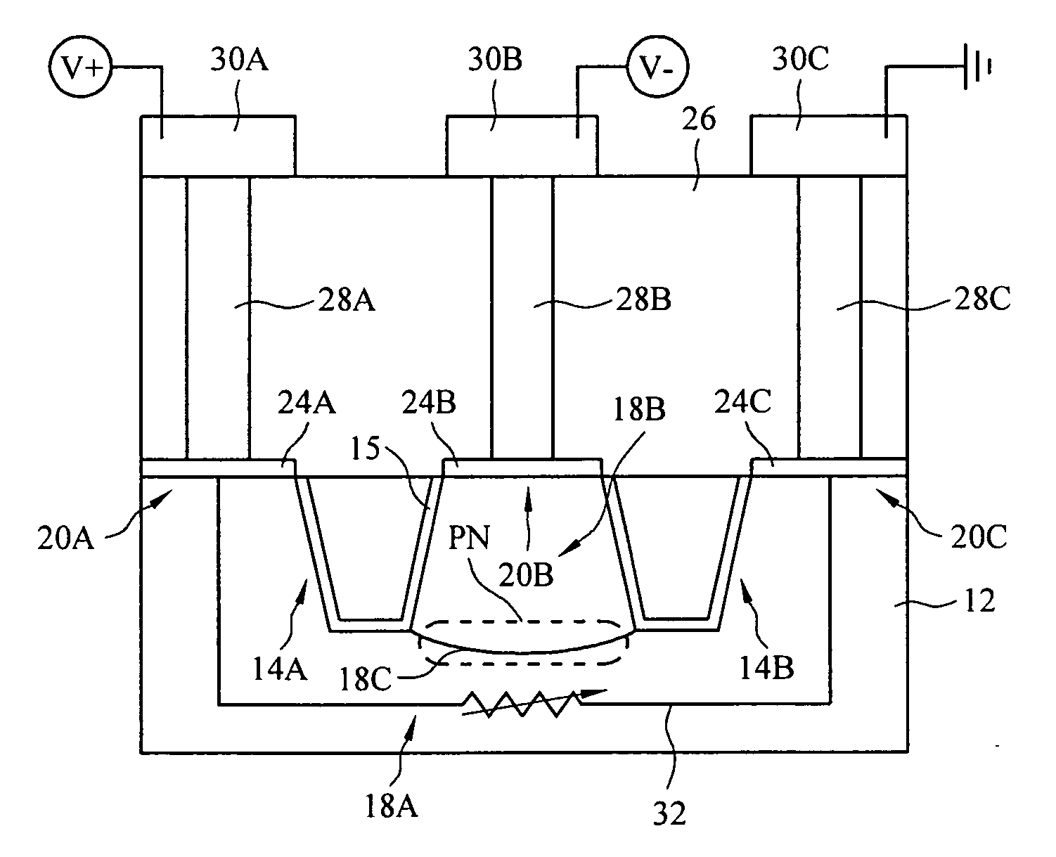
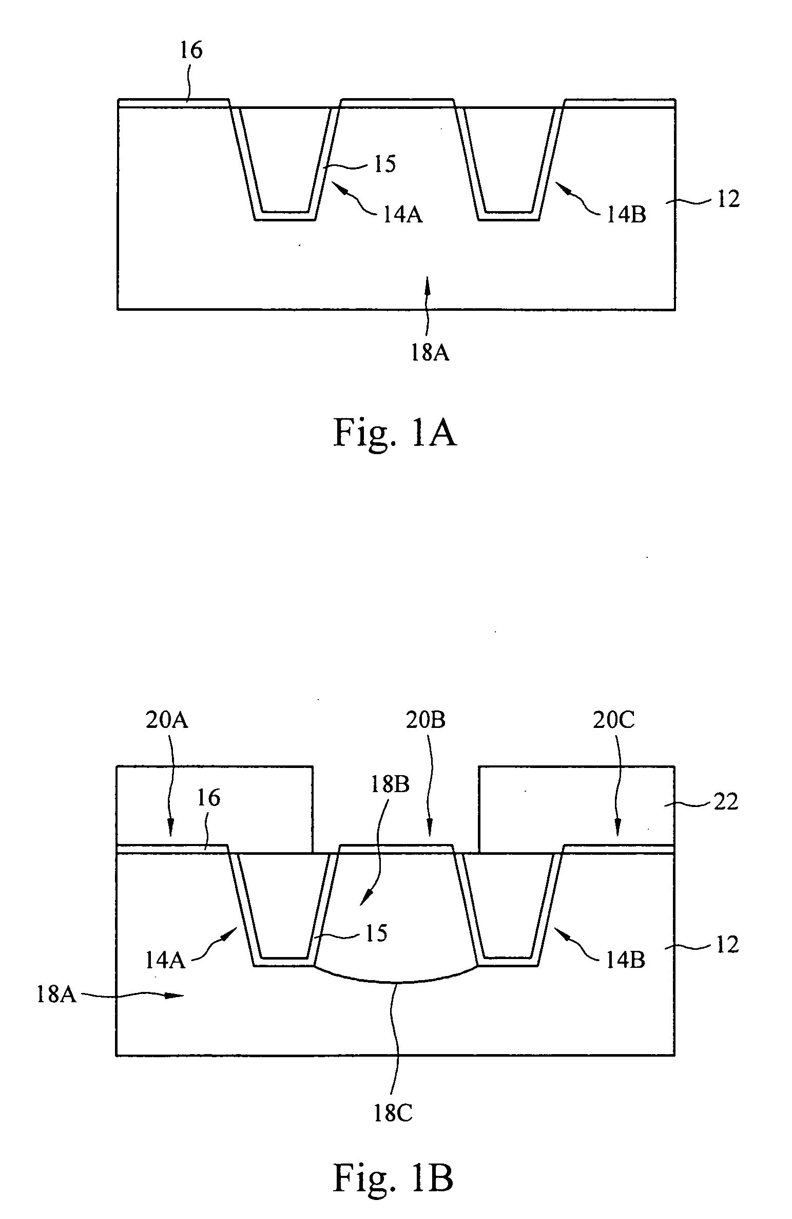
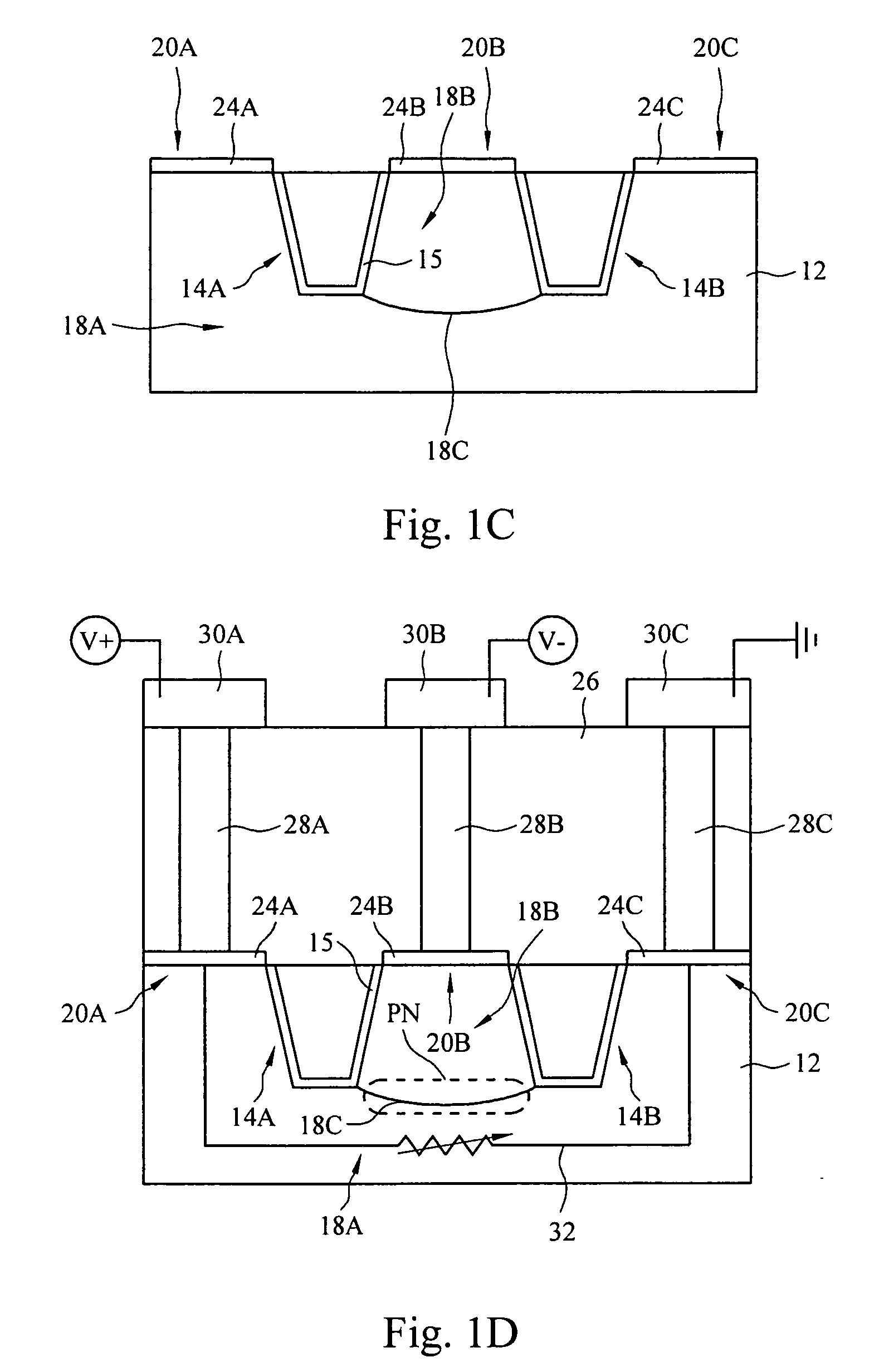
[0012] Although the method of the present invention is explained with reference to formation of an exemplary dummy substrate pattern it will be appreciated that the spacing of the dummy pattern, e.g., dummy shallow trench isolation (STI) isolation regions, may be varied as required to provide an appropriate pattern density to improve a CMP polishing process of active regions, for example avoiding a dishing effect when forming STI isolation regions in active regions. It will also be appreciated that dummy regions including the dummy STI structures and intervening mesa structures may be placed surrounding or adjacent active regions including conventional semiconductor devices including logic devices and mixed signal (digital / analog) devices.

[0013] Referring to FIG. 1A, is shown a dummy region portion of semiconductor substrate 12. For example, the substrate 12 may include, but is not limited to, silicon, silicon on insulator (SOI), stacked SOI (SSOI), stacked SiGe on insulator (S-SiG...


PUM


Abstract

A dummy region varactor for improving a CMP process and improving electrical isolation from active areas and a method for forming the same, the varactor including a semiconductor substrate having a dummy region said dummy region including a first well region having a first polarity; shallow trench isolation (STI) structures disposed in the dummy region defining adjacent mesa regions comprising first, second, and third mesa regions; a second well region having a second polarity underlying the first mesa region having the second polarity to form a PN junction interface; wherein said second and third mesa regions having the first polarity are formed adjacent either side of said first mesa region.

Description

FIELD OF THE INVENTION [0001] This invention generally relates to integrated circuit device manufacturing and more particularly to dummy substrate patterns for improving CMP processes including formation of an adjustable varactor formed within the dummy pattern for use in logic and mixed signal applications. BACKGROUND OF THE INVENTION [0002] During STI formation, CMP of an overlying STI oxide layer in the formation of STI structures generally leads to dishing or preferential polishing of the upper portion of the STI structure in relation to surrounding surfaces. [0003] In addition, in logic and mixed signal operations, device elements such as resistors are formed in an active device area. Prior art methods have proposed forming dummy areas surrounding active areas to avoid dishing effects in CMP processes to form STI structures as well as improve the uniformity in polysilicon e.g., gate electrode etching processes. [0004] However, a problem in the prior art is that the formation of...

Claims


Application Information

Patent Timeline
IPC IPC(8): H01L29/93
CPCH01L27/0808H01L29/93H01L29/417
Inventor CHENG, CHUNG-LONGTHEI, KONG-BENGLIN, SHENG-YUAN
Owner TAIWAN SEMICON MFG CO LTD
Why Eureka
Try Eureka