Chemical mechanical polishing process

a technology of mechanical polishing and chemical polishing, applied in the direction of lapping machines, metal-working apparatus, electrical equipment, etc., can solve the problems of affecting tool uptime and product throughput, difficult to construct an optical pathway for continuous light transmission, and short life of the politex soft pad applicable to the barrier cmp,

Active Publication Date: 2007-05-17
MARLIN SEMICON LTD
View PDF10 Cites 5 Cited by
  • Summary
  • Abstract
  • Description
  • Claims
  • Application Information

AI Technical Summary

Benefits of technology

[0012] It is therefore a primary objective of the present invention to provide an improved copper / barrier CMP process to solve the above-described prior art problems.

Problems solved by technology

Because both the surface being polished and the polishing pad are in continuous motion during the polishing process, it is difficult to construct an optical pathway for continuous light transmission.
However, the above-described prior art copper / barrier CMP utilizing a soft pad for barrier polishing has some drawbacks.
First, the lifetime of the Politex soft pad applicable for the barrier CMP is very short (˜10 hours).
Frequent change of the Politex soft pad on the second platen adversely affects the tool uptime and product throughput.
Second, when using the Politex soft pad on the third platen, the removal rate of the barrier layer is unstable and the uniformity is not satisfactory.
The unstable removal rate and poor uniformity due to the use of the Politex soft pad deteriorate as the pad is near the end of its lifetime.

Method used


Image

  • Chemical mechanical polishing process
  • Chemical mechanical polishing process
  • Chemical mechanical polishing process

Examples


Embodiment Construction

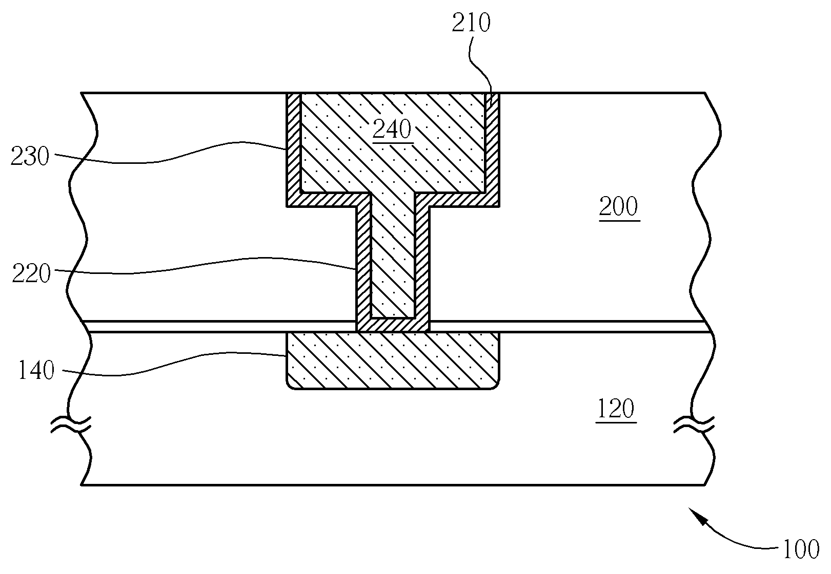
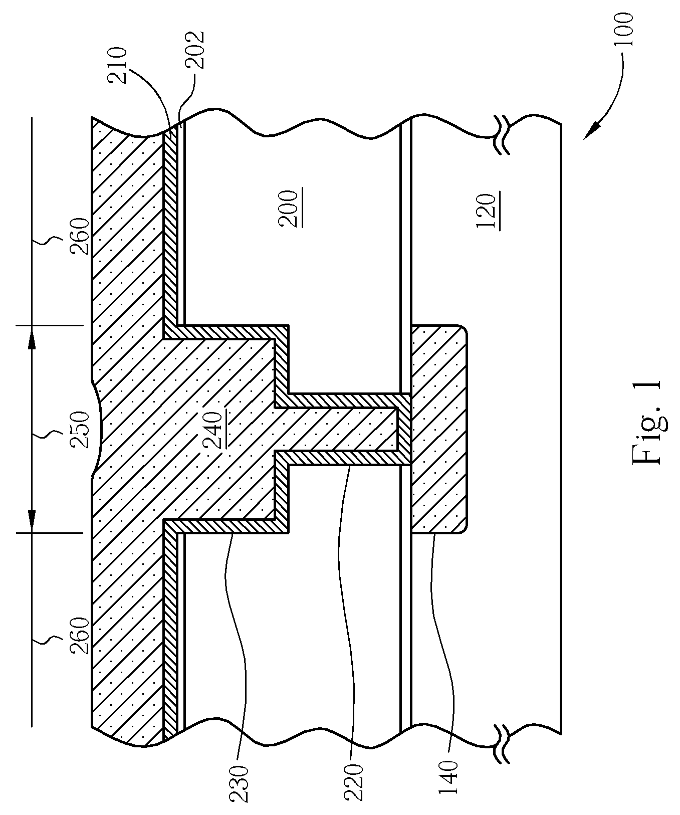
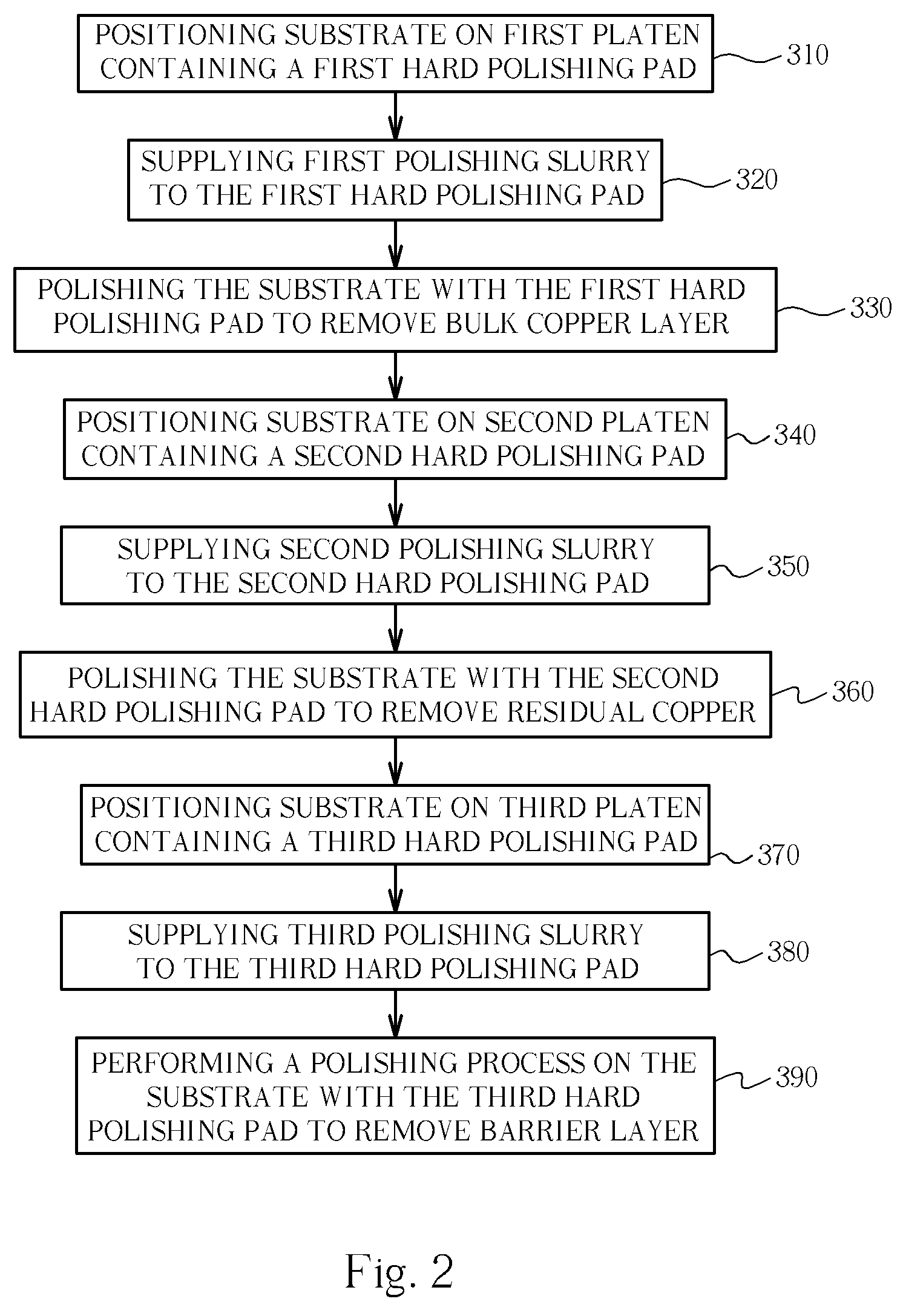
[0020] The present invention is directed to a method of forming reliable interconnects of integrated circuits, more specifically to a copper / barrier chemical mechanical polishing process applied during the back end fabrication of integrated circuits with inlaid copper interconnects. In general, aspects of the invention provide methods for planarizing a substrate surface using multiple hard polishing pads while minimizing scratching and defects of the substrate surface.

[0021] The invention will be described below in reference to a planarizing process for the removal of conductive materials, such as copper containing materials, and barrier layer materials, such as tantalum and tantalum nitride, from a substrate surface by chemical mechanical polishing (CMP) techniques with hard polishing pads.

[0022] It is to be understood that the term “copper layer” used hereinafter means copper or any suitable copper alloys known in the art unless otherwise indicated. The advantages of this invent...


PUM

PropertyMeasurementUnit
flow rateaaaaaaaaaa
pressureaaaaaaaaaa
pHaaaaaaaaaa

Abstract

A copper/barrier CMP process includes (a) providing a substrate having a bulk metal layer and a barrier layer; (b) polishing the substrate with a first hard polishing pad on a first platen to substantially remove an upper portion of the bulk metal layer, wherein the first hard polishing pad has a hardness of above 50 (Shore D); (c) polishing the substrate with a second hard polishing pad on a second platen to remove residual copper, thereby exposing the barrier layer, wherein the second hard polishing pad has a hardness of above 50 (Shore D); and (d) polishing the substrate with a third hard polishing pad on a third platen to remove the barrier layer, wherein the third hard polishing pad has a hardness ranging between 40-50 (Shore D).

Description

BACKGROUND OF THE INVENTION [0001] 1. Field of the Invention [0002] The present invention relates to the field of semiconductor fabrication, and more particularly, to chemical mechanical polishing and planarization of semiconductor devices. [0003] 2. Description of the Prior Art [0004] The increasing need to form planar surfaces on a variety of materials has led to the development of process technology known as chemical mechanical polishing (CMP). The CMP method typically requires that the substrate be mounted on a carrier or polishing head. The exposed surface of the substrate is placed against a rotating polishing pad. The polishing pad may be either a “standard” pad or a fixed-abrasive pad. A fixed-abrasive pad has abrasive particles held in a containment media, whereas a standard pad has a durable surface, without embedded abrasive particles. The carrier head provides a controllable load, i.e., pressure, on the substrate to push it against the polishing pad. Polishing slurry, in...

Claims


Application Information

Patent Timeline
Patent Type & Authority Applications(United States)
IPC IPC(8): H01L21/4763H01L21/461H01L21/302
CPCB24B37/042H01L21/3212H01L21/7684
Inventor NEO, BOON-TIONGLIN, CHIN-KUNLAU, LEE-LEE
Owner MARLIN SEMICON LTD
Why Eureka
Try Eureka