Pad conditioner for conditioning a cmp pad and method of making such a pad conditioner

a conditioner and pad technology, applied in the field of pad conditioners, can solve the problems of reducing the removal rate of polishing, reducing and reducing so as to enhance the stability of the cmp process, prolong the life of polishing pads, and improve the efficiency and uniformity of pad conditioners

Inactive Publication Date: 2007-02-15
PRINCO CORP
View PDF36 Cites 15 Cited by
  • Summary
  • Abstract
  • Description
  • Claims
  • Application Information

AI Technical Summary

Benefits of technology

[0022] Through the invention, the efficiency and uniformity of the pad conditioner are improved, and the life of the polishing pad is extended. Moreover, the invention can enhance the stability of CMP process, reduce the conditioning time, minimize the number and time of equipment maintenances, and reduce the generation of scratched wafers, thus enhancing the quality and yield of wafers.

Problems solved by technology

Therefore, although the majority of debris coming from the polishing of silicon wafers, slurry particles and conditioning disk is washed away by water during the CMP process, a small amount of debris still accumulates in the via holes of the polishing pad, causing the polishing pad surface to glaze or harden, which makes the pad less able to hold the slurry particles.
Thus the removal rate of polishing is decreased, which causes instability in the CMP process and fast wear-out of the polishing pad.
The abrasive particles of the electroplated pad conditioner are fixed on its substrate by way of electroplating nickel, but the bonding force of such mechanical locking method is poor and the abrasive particles tend to be dislodged easily and may scratch the wafer being polished.
Furthermore, the electroplated layer must cover more than half of each abrasive particle in order to engage the abrasive particles to the substrate, therefore the protrusion level of the abrasive particles is limited, and thus the polishing pad cannot be effectively conditioned and the via holes are stuffed with the debris.
However, there are some disadvantages, one of them being uneven distribution of particles on the substrate, which may result from the unevenness of spacing between abrasive particles or the unevenness of the level of height where the abrasive particles exist.
Both of the unevenness causes the abrasive particles to apply uneven forces to the polishing pad, which in turn will cause the abrasive particles that bear bigger force to be wholly dislodged or partly chipped easily, thereby leading to scratching of the wafers.
In addition, if the spacing between the distributed abrasive particles is too close, the debris would accumulate easily, and the work efficiency of the pad conditioner would be reduced.
Besides, an excessive amount of accumulated debris will easily scratch the wafer once they fall off.

Method used


Image

  • Pad conditioner for conditioning a cmp pad and method of making such a pad conditioner
  • Pad conditioner for conditioning a cmp pad and method of making such a pad conditioner
  • Pad conditioner for conditioning a cmp pad and method of making such a pad conditioner

Examples


Embodiment Construction

[0029] A pad conditioner for conditioning a CMP pad and a method of making such a pad conditioner according to a preferred embodiment of the invention will be described below with reference to the drawings, wherein the like reference numerals denote the like components. Please note that the embodiments of the invention described below are for explanatory purposes and are not limited to the description thereof unless such limitation is specified in the embodiments.

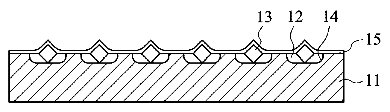
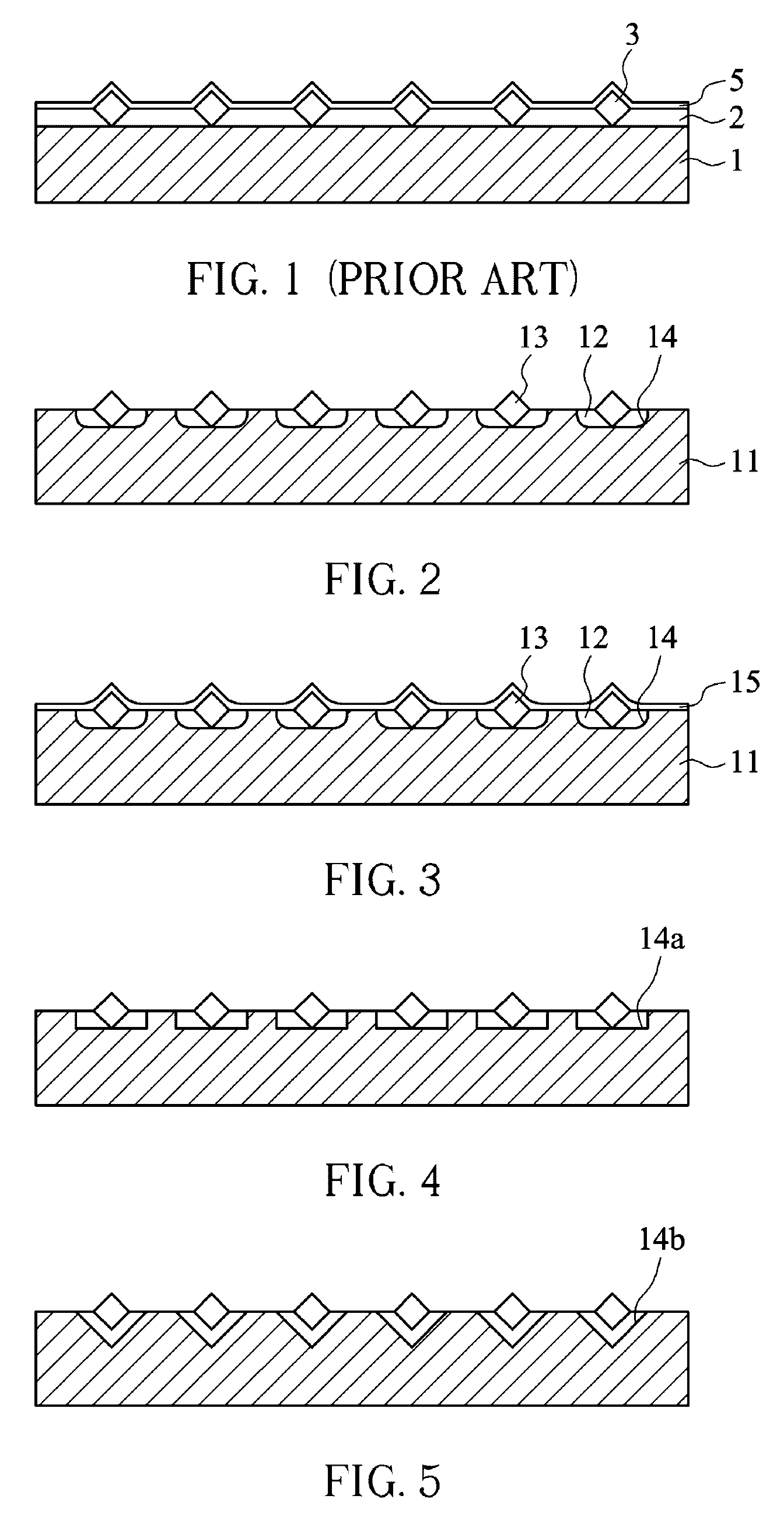
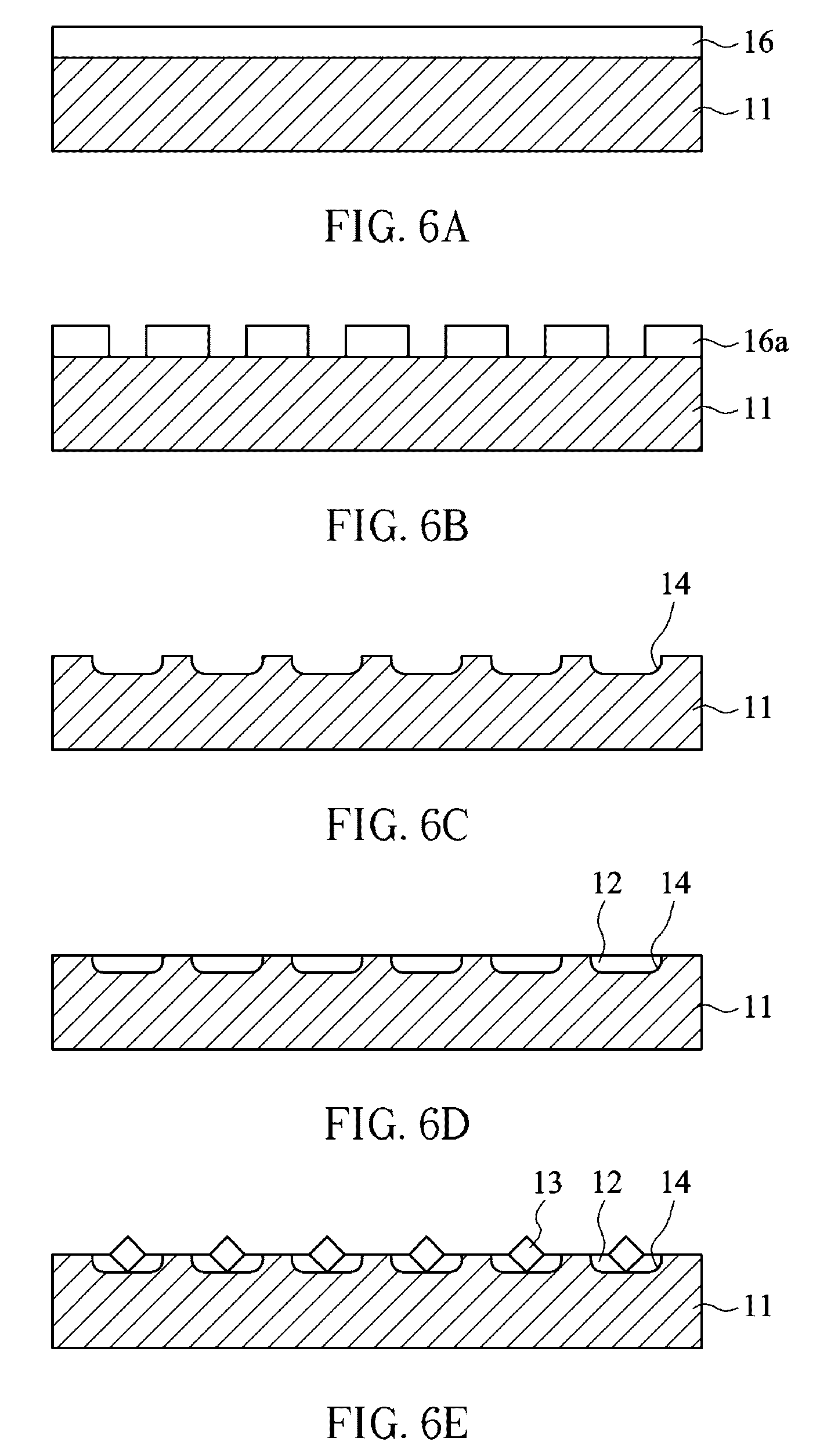
[0030] Referring to FIG. 2, a sectional view of a pad conditioner according to a first embodiment of the invention is disclosed, wherein a plurality of abrasive particles 13 are respectively fixed in a plurality of flat-bottom, bowl-shaped cavities 14 on a substrate 11 by a bonding agent 12. In this embodiment, the substrate 11 is made of stainless steel SUS 316, and the sizes of the abrasive particles are from about 100 μm to about 250 μm, preferably about 130 μm to about 200 μm. The depth of the cavities 14 is about 50 μ...


PUM

PropertyMeasurementUnit
sizesaaaaaaaaaa
sizesaaaaaaaaaa
depthaaaaaaaaaa

Abstract

The invention provides a pad conditioner for conditioning a CMP pad. The pad conditioner includes a substrate, a plurality of cavities on the substrate, a bonding agent filling in the cavities, and a plurality of abrasive particles securely placed and fixed in the cavities separately. The cavities are arranged in a regular manner and each cavity is sized such that it can accommodate only one abrasive particle. The cavities may be bowl-shaped or of other shapes. A method of making such a pad conditioner is also disclosed.

Description

BACKGROUND [0001] 1. Field of the Invention [0002] The present invention relates to a pad conditioner for dressing or conditioning a CMP pad and a method of making such a pad conditioner, and more particularly to a pad conditioner for conditioning a CMP pad and a method of making such a pad conditioner wherein abrasive particles are evenly distributed on the pad conditioner and securely fixed on a substrate. [0003] 2. Description of the Related Art [0004] In current semiconductor manufacturing processes, as the manufacturing technology advances, the line width and die size become smaller, and interconnections more concentrated and need to be stacked into more layers. Thus the planarization of the wafer becomes important, and Chemical Mechanical Polishing (CMP) is the key technology that provides global planarization. [0005] In CMP, a silicon wafer is held by a rotating or moving polishing head and pressed on a rotating polishing pad, and slurry is injected onto the polishing pad. Be...

Claims


Application Information

Patent Timeline
Patent Type & Authority Applications(United States)
IPC IPC(8): B24B1/00B24B21/18B24B53/017B24B53/12B24D3/00B24D7/00H01L21/304
CPCB24D18/0027B24B53/017
Inventor SHIH, YING-CHE
Owner PRINCO CORP
Why Eureka
Try Eureka