
Bump land structure of circuit substrate for semiconductor package

a technology of circuit substrate and bump land, which is applied in the direction of resist details, printed circuit aspects, printed circuit manufacturing, etc., can solve the problem of reducing the reliability of bump land

Inactive Publication Date: 2006-10-05
SAMSUNG ELECTRONICS CO LTD
View PDF8 Cites 11 Cited by
  • Summary
  • Abstract
  • Description
  • Claims
  • Application Information

AI Technical Summary

Benefits of technology

The present invention provides a circuit substrate with a bump land structure that includes a lower layer, an intermediate layer, and an upper layer. A solder mask is provided to cover the entire peripheral region of the lower layer. The bump land structure is designed to improve the reliability and stability of the circuit substrate. The technical effects of the invention include improved mounting and soldering of components on the circuit substrate, as well as increased reliability and stability of the overall circuit assembly.

Problems solved by technology

The neck shape may reduce bump joint reliability.

Method used


Image

  • Bump land structure of circuit substrate for semiconductor package
  • Bump land structure of circuit substrate for semiconductor package
  • Bump land structure of circuit substrate for semiconductor package

Examples


Embodiment Construction

[0033] Example, non-limiting embodiments of the present invention will now be described more fully hereinafter with reference to the accompanying drawings. This invention may, however, be embodied in many different forms and should not be construed as limited to the example embodiments set forth herein. Rather, the disclosed embodiments are provided so that this disclosure will be thorough and complete, and will fully convey the scope of the invention to those skilled in the art. The principles and feature of this invention may be employed in varied and numerous embodiments without departing from the scope of the invention.

[0034] Well-known structures and processes are not described or illustrated in detail to avoid obscuring embodiments of the present invention.

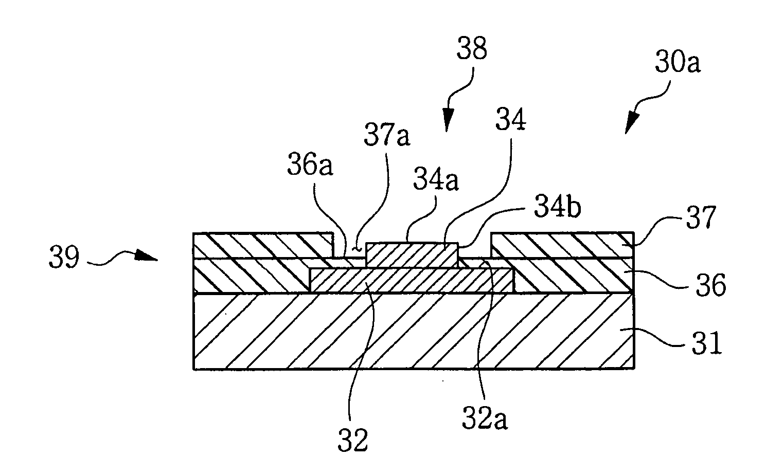
[0035]FIG. 6 is a plan view of a bump land structure 30a of a circuit substrate in accordance with an example, non-limiting embodiment of the present invention. FIG. 7 is a cross-sectional view taken along the line of VII-...


PUM


Abstract

A bump land structure of a circuit substrate for a semiconductor package may have a combination of an SMD type bump land structure and an NSMD type bump land structure. A lower portion of a solder mask and a lower layer of a bump land may form the SMD type bump land structure. An upper portion of a solder mask and an upper layer of a bump land may form the NSMD type bump land structure.

Description

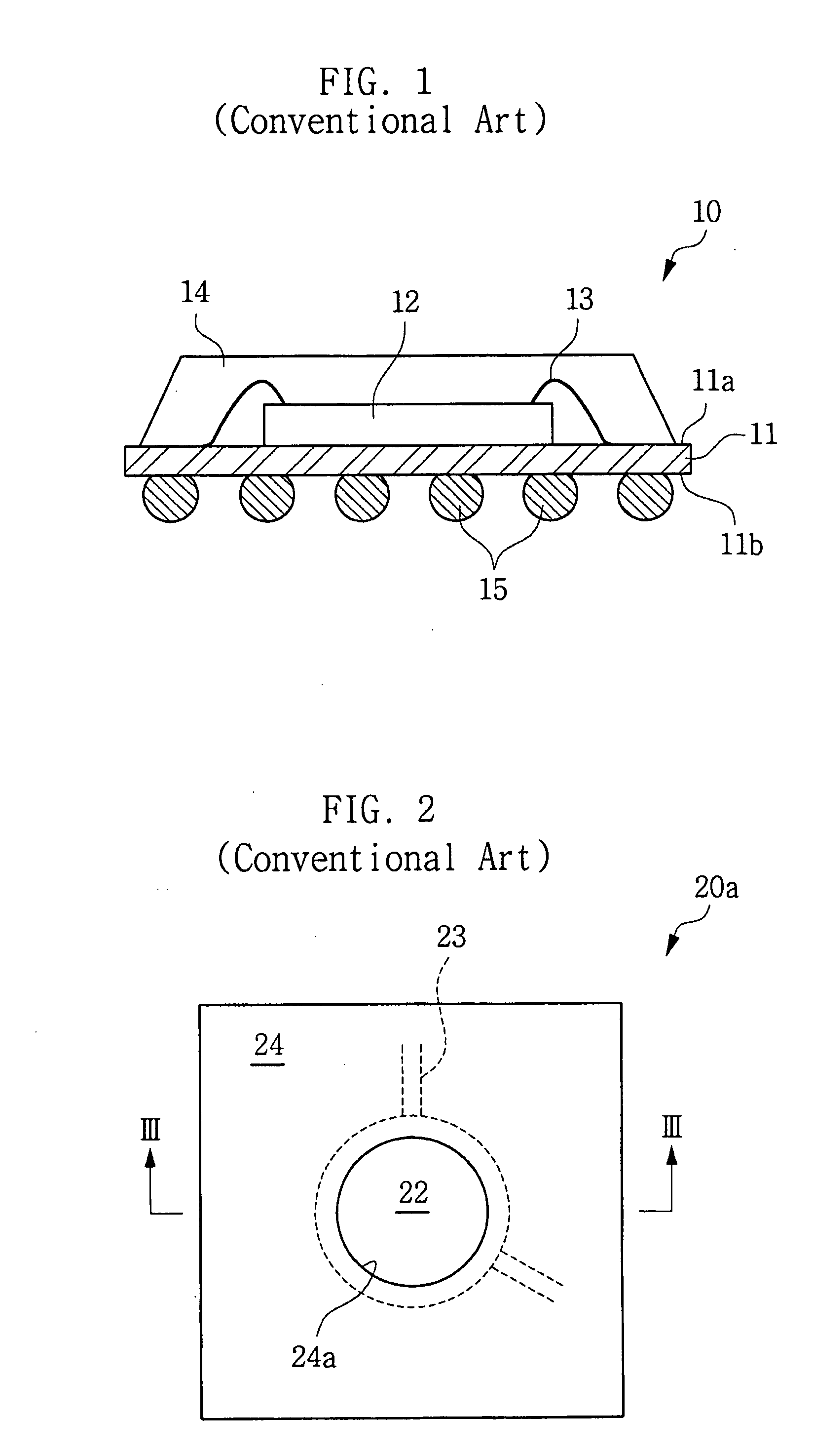
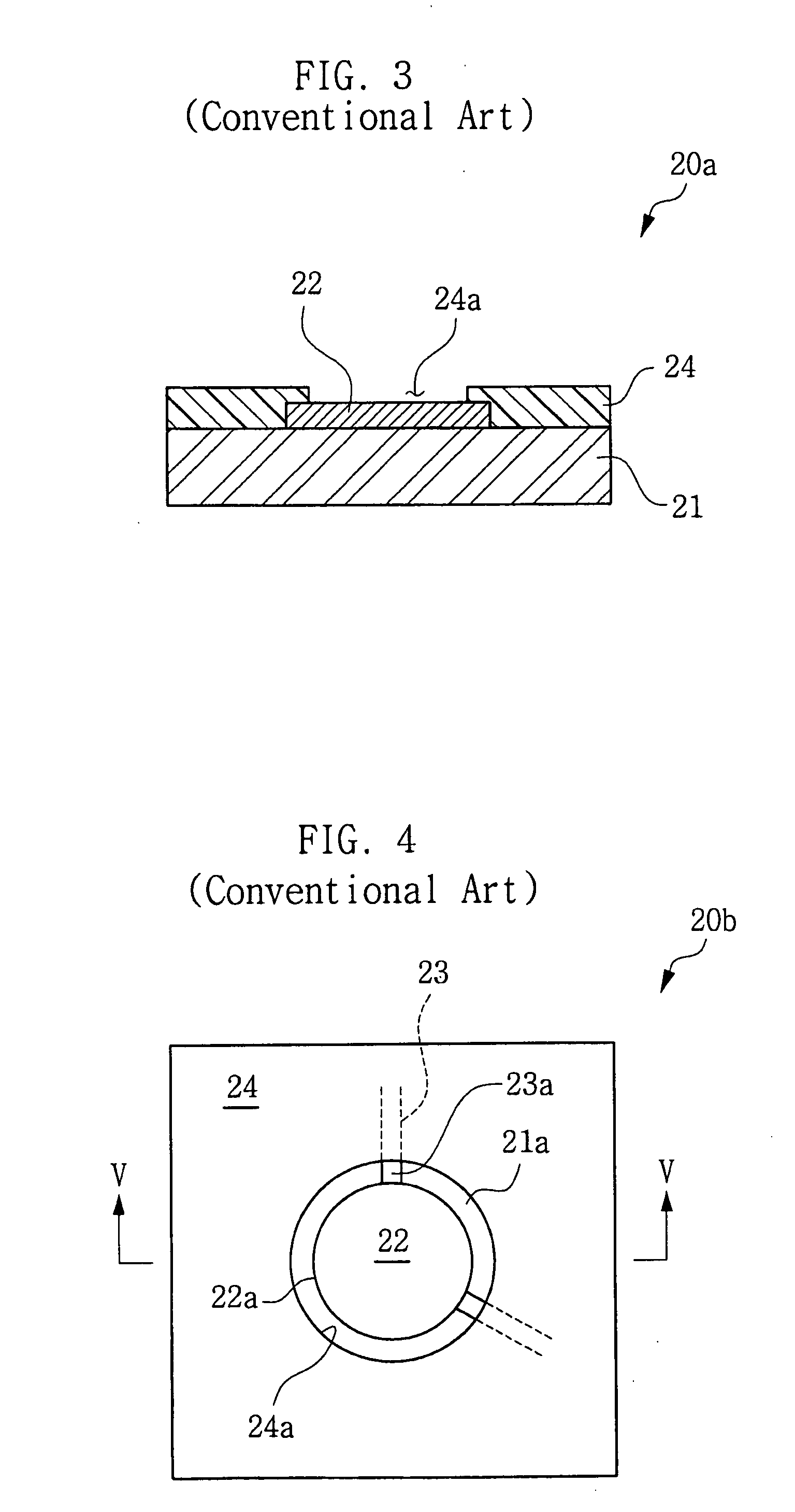
PRIORITY STATEMENT [0001] This U.S. non-provisional application claims priority under 35 U.S.C. § 119 from Korean Patent Application No. 2004-102367, filed on Dec. 7, 2004, the entire contents of which are incorporated herein by reference. BACKGROUND OF THE INVENTION [0002] 1. Field of the Invention [0003] The present invention relates generally to circuit substrates for semiconductor packages and, more particularly, to bump land structures of circuit substrates. [0004] 2. Description of the Related Art [0005] Integration technology for integrated circuits (ICs) may make it possible to connect many circuits in and on a semiconductor chip at a given chip size. Thus, a package, which contains the semiconductor chip therein, may have many input / output (I / O) terminals communicating with external circuitry such as a motherboard, for example. [0006] A ball grid array (BGA) package may have I / O terminals distributed over a package surface, rather than just located peripherally at one or mo...

Claims


Application Information

Patent Timeline
Patent Type & Authority Applications(United States)
IPC IPC(8): H01L23/48
CPCH01L23/49816H05K1/111H05K3/243H05K3/3452H05K3/4007H01L2924/15311H05K2201/09436H05K2201/09845H05K2203/0594H01L2224/48227H05K2201/0367H01L23/12H01L21/60
Inventor KIM, KIL-SOOJUNG, IN-SOOK
Owner SAMSUNG ELECTRONICS CO LTD
Learn More