Semiconductor device and an image sensing device

a technology of image sensing and semiconductors, applied in the field of semiconductor devices, can solve problems such as boosted coupling nois

Inactive Publication Date: 2006-10-05
RENESAS ELECTRONICS CORP
View PDF3 Cites 40 Cited by
  • Summary
  • Abstract
  • Description
  • Claims
  • Application Information

AI Technical Summary

Benefits of technology

[0023] Thus, SI can be improved in a semiconductor device in which a plurality of semiconductor chips differing in withstand voltage or a plurality of semiconductor chips differing in noise immunity, such as a multi-chip module.

Problems solved by technology

If this arrangement is to satisfy the requirement for simplified wiring structure of the mother board, it is desirable to allocate an outermost ball electrode for that external terminal for analog signals on the array, but this might sometimes invite boosted coupling noise due to increased wiring within the substrate.

Method used


Image

  • Semiconductor device and an image sensing device
  • Semiconductor device and an image sensing device
  • Semiconductor device and an image sensing device

Examples


Embodiment Construction

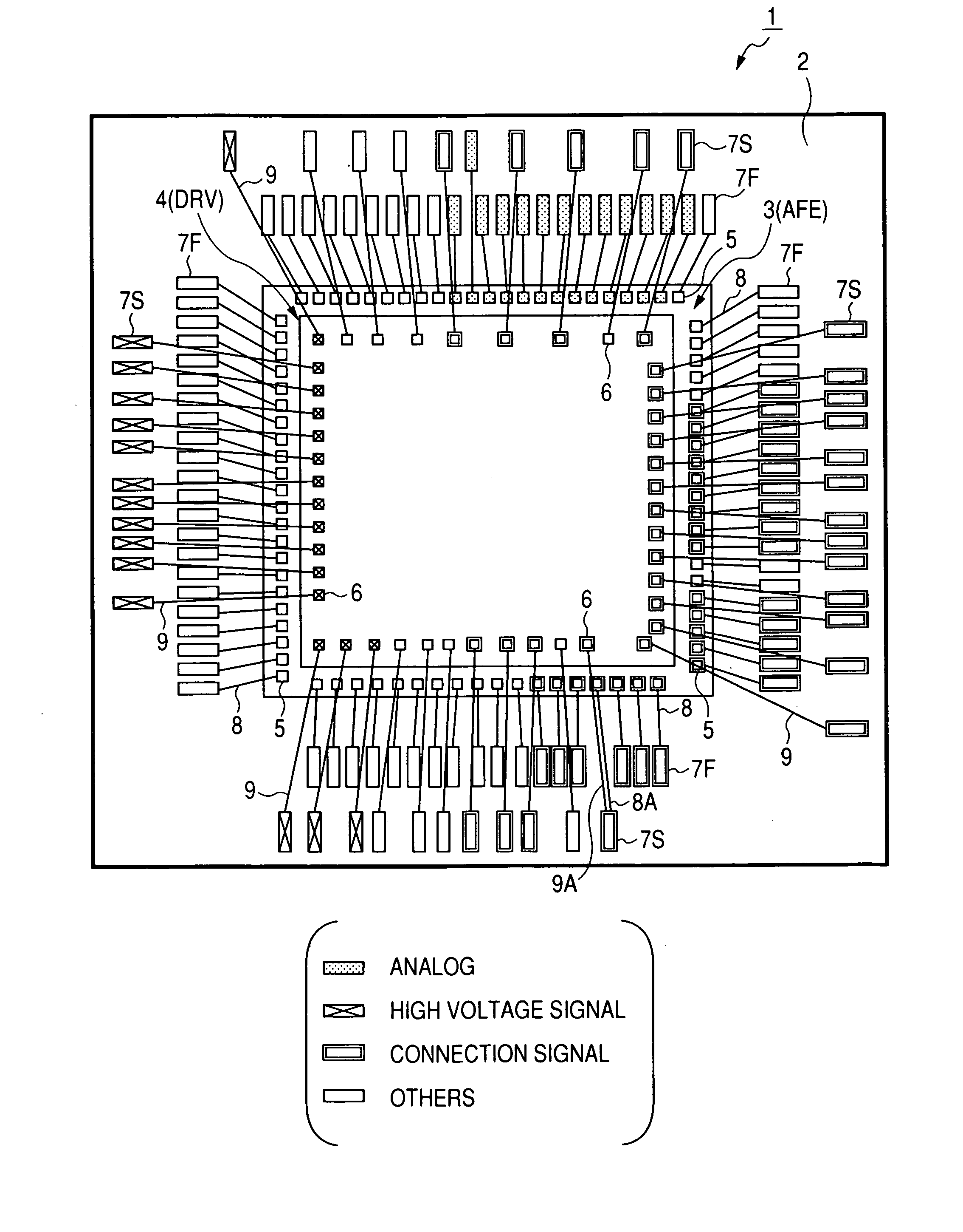
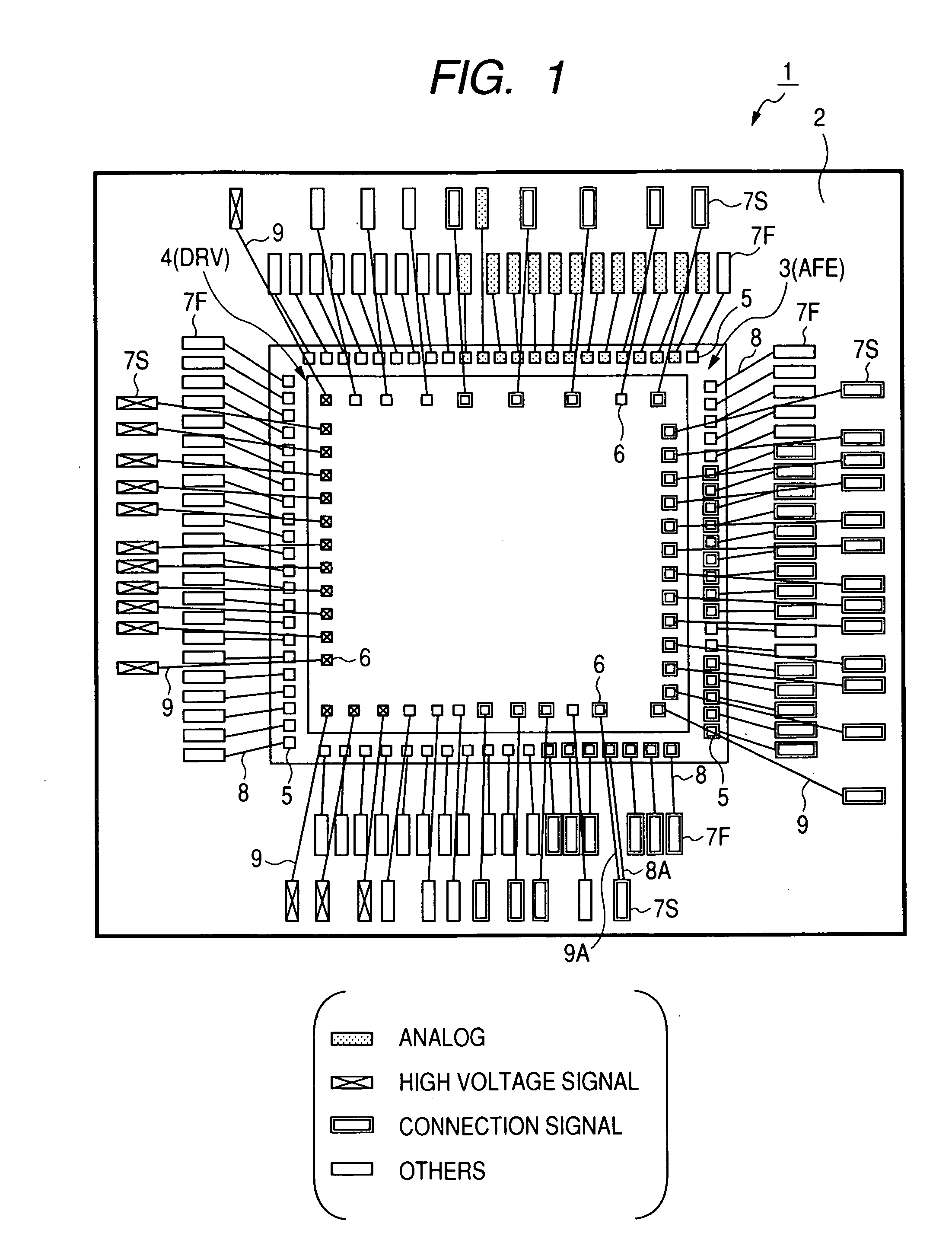
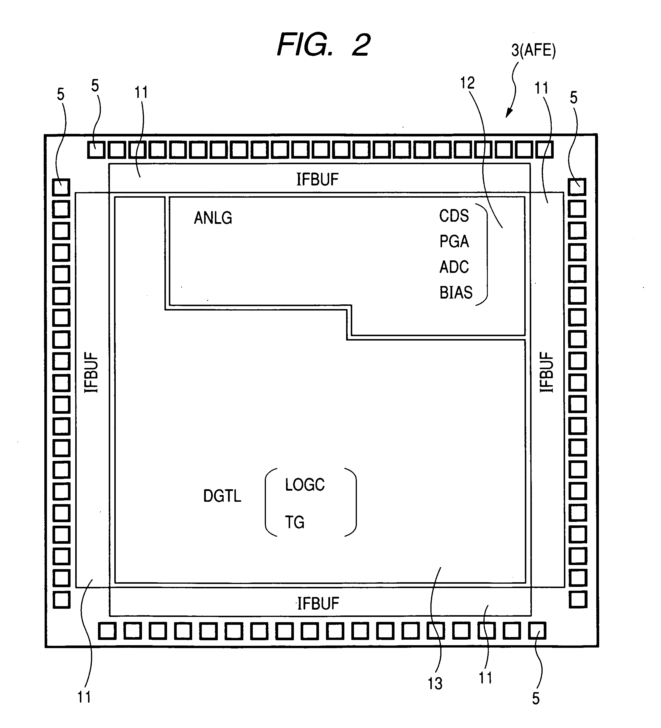
[0041]FIG. 1 is a broad plan illustrating a semiconductor device. A semiconductor device 1 has a CCD analog front end chip (AFE) 3 as a first semiconductor chip and a CCD driver chip (DRV) 4 as a second semiconductor chip over a package substrate 2. Over the CCD analog front end chip (AFE) 3 bonding pads 5 are arranged in a row along the edge of each side, and over the CCD driver chip (DRV) 4 bonding pads 6 are arranged in a row along the edge of each side. Over the package substrate 2, bonding pads 7 are arranged in two rows along the edge of each side. The second row of the bonding pads 7 (second bonding pads) 7S is arranged closer to an edge of the package substrate 2 than the first row (first bonding pads) 7F. The first bonding pads 7F are bonded to the bonding pads 5 of the CCD analog front end chip 3 by bonding wires 8. The second bonding pads 7S are bonded to the bonding pads 6 of the CCD driver chip 4 by bonding wires 9. As represented by 8A and 9A, there also is a form of c...


PUM


Abstract

SI in a semiconductor device in which a plurality of semiconductor chips differing in withstand voltage or in noise immunity, such as a multi-chip module, is to be improved. The semiconductor device comprises a first semiconductor chip and a second semiconductor chip mounted over a package substrate which has a plurality of bonding pads arranged along the edges. The first semiconductor chip has a plurality of bonding pads for analog signals, and the second semiconductor chip has a plurality of bonding pads for high-voltage signals. The edges along which the bonding pads for analog signals are arranged and the edges along which the bonding pads for high-voltage signals are arranged are disposed along mutually different edges of the package substrate. Adjoining of electrodes or wirings for high voltage signals and those for analog signals over the package substrate can be easily avoided, and SI deterioration can be thereby restrained.

Description

CROSS REFERENCE TO RELATED APPLICATION [0001] The present application claims priority from Japanese Patent Application No. 2005-103102 filed on Mar. 31, 2005, the content of which is hereby incorporated by reference into this application. BACKGROUND OF THE INVENTION [0002] The present invention relates to a semiconductor device in which a plurality of semiconductor chips differing in withstand voltage or a plurality of semiconductor differing in chip noise immunity are stacked one over another, such as a multi-chip module (MCM). More particularly, it relates to a technique which can be effectively applied to system-in-package (SIP) semiconductor devices which perform, for instance, analog front end processing for the outputs of charge-coupled devices (CCDs) and pulse driving for CCDs. [0003] Known multi-chip modules in which a plurality of semiconductor chips differing in noise immunity are stacked one over another include one in which individually formed analog chips and digital ch...

Claims


Application Information

Patent Timeline
Patent Type & Authority Applications(United States)
IPC IPC(8): H03K17/16
CPCH01L23/498H01L23/49838H01L23/50H01L24/45H01L24/49H01L27/14618H01L27/14634H01L2224/45144H01L2224/48091H01L2224/48227H01L2224/48465H01L2224/49171H01L2224/49433H01L2224/85444H01L2225/0651H01L2225/06527H01L2225/06575H01L2225/06586H01L2924/01004H01L2924/01005H01L2924/01014H01L2924/01015H01L2924/01028H01L2924/01029H01L2924/01038H01L2924/01079H01L2924/14H01L2924/15311H01L2924/19041H01L2924/19042H01L2924/19043H01L2924/30105H01L2924/3025H01L24/48H01L2924/01006H01L2924/01023H01L2924/01033H01L2924/014H01L2224/32145H01L2224/32225H01L2224/73265H01L2924/00014H01L2924/00H01L2924/00012H01L2224/48644H01L24/73H01L2924/181H01L2224/05553H01L2224/05554
Inventor HIRANUMA, KAZUHIKOKURODA, HIROSHIABE, YOSHIYUKI
Owner RENESAS ELECTRONICS CORP
Why Eureka
Try Eureka