Masking of repeated overlay and alignment marks to allow reuse of photomasks in a vertical structure
- Summary
- Abstract
- Description
- Claims
- Application Information
AI Technical Summary
Benefits of technology
Problems solved by technology
Method used
Image

Examples
example
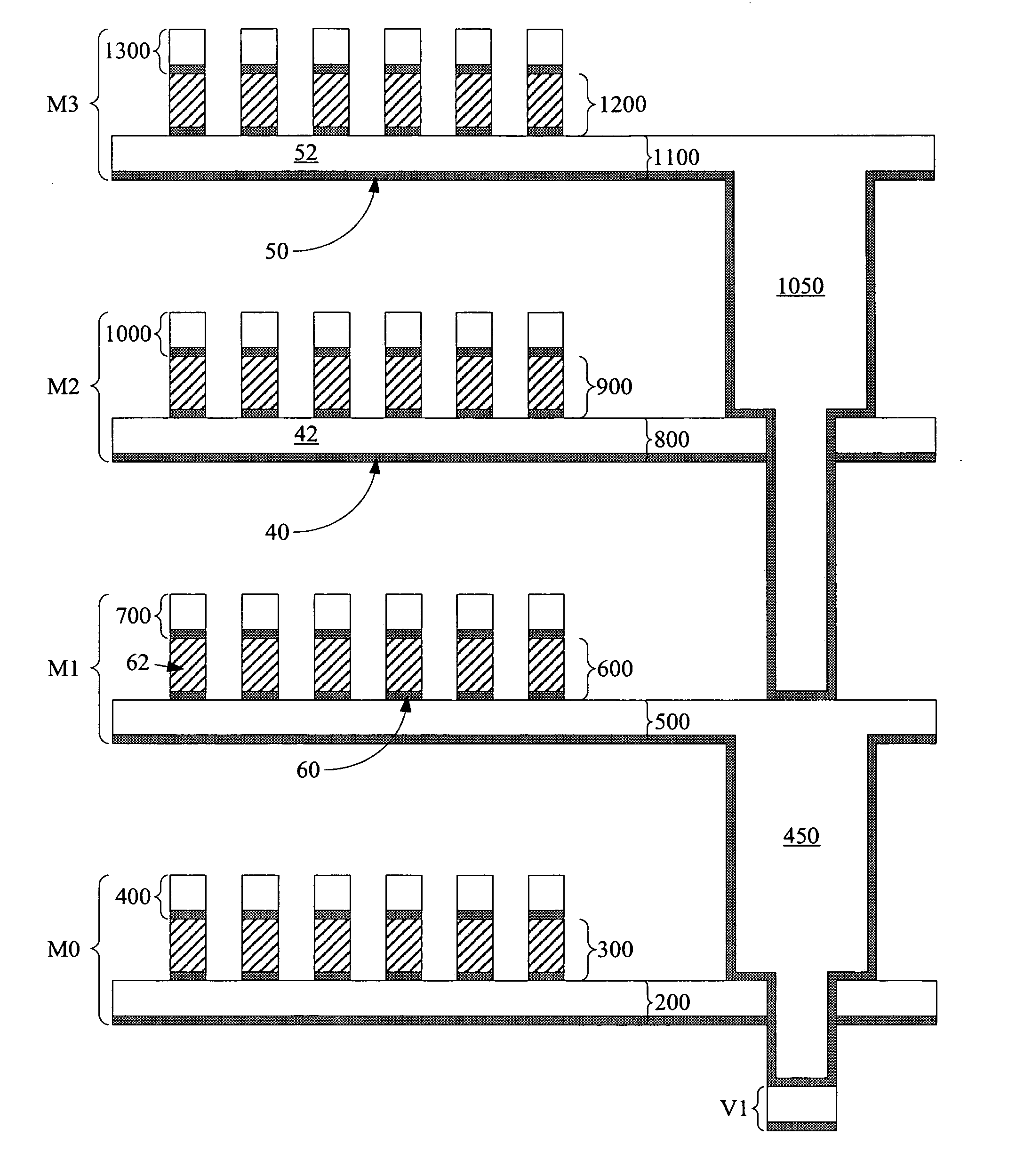
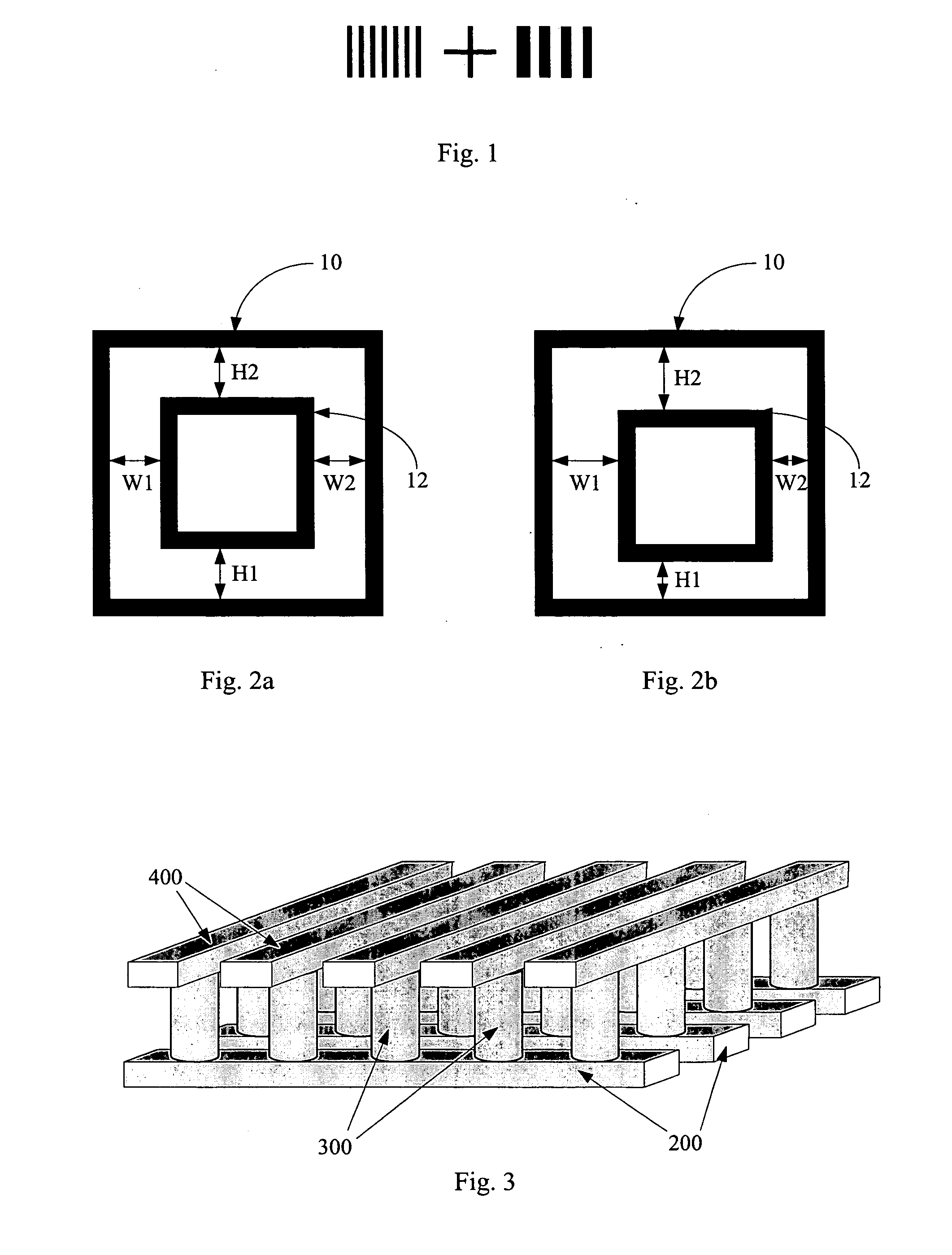
[0053]FIG. 7 is a cross-sectional view of a monolithic three dimensional memory array having four stacked memory levels. It will be understood that such a memory array could have more memory levels or fewer.
[0054] Fabrication begins with a substrate, preferably a monocrystalline silicon wafer. Before formation of memory levels begins, routing layers are formed above the substrate, including routing layer V1. (For simplicity, not all routing layers are shown.) A conductor photomask, Y0, is used to form bottom conductors 200 of memory level M0. A pillar photomask, BC0, is used to form pillars 300 of memory level M0, and another conductor photomask, X1, is used to form top conductors 400, completing memory level M0. Each of these photomasks is unique. (Names like Y0, BC0, and X1 are used to refer to unique photomasks for clarity, and these names will appear in charts in FIGS. 8 and 9. FIG. 7, however, shows the structures formed, not the photomasks used to form them; thus the photomas...
PUM
 Abstract
Description
Claims
Application Information