Assisting printed board design process

Inactive Publication Date: 2006-10-05
RICOH KK
View PDF2 Cites 4 Cited by
  • Summary
  • Abstract
  • Description
  • Claims
  • Application Information

AI Technical Summary

Benefits of technology

[0004] In light of the above-described and other problems, there is a need for a printed board design process capable of selecting a board material or a board sheet in a more efficient manner. Further, the board material selection or the board sheet selection s

Problems solved by technology

However, the board material selection or the board sheet selection can be cumbersome

Method used


Image

  • Assisting printed board design process
  • Assisting printed board design process
  • Assisting printed board design process

Examples


Example

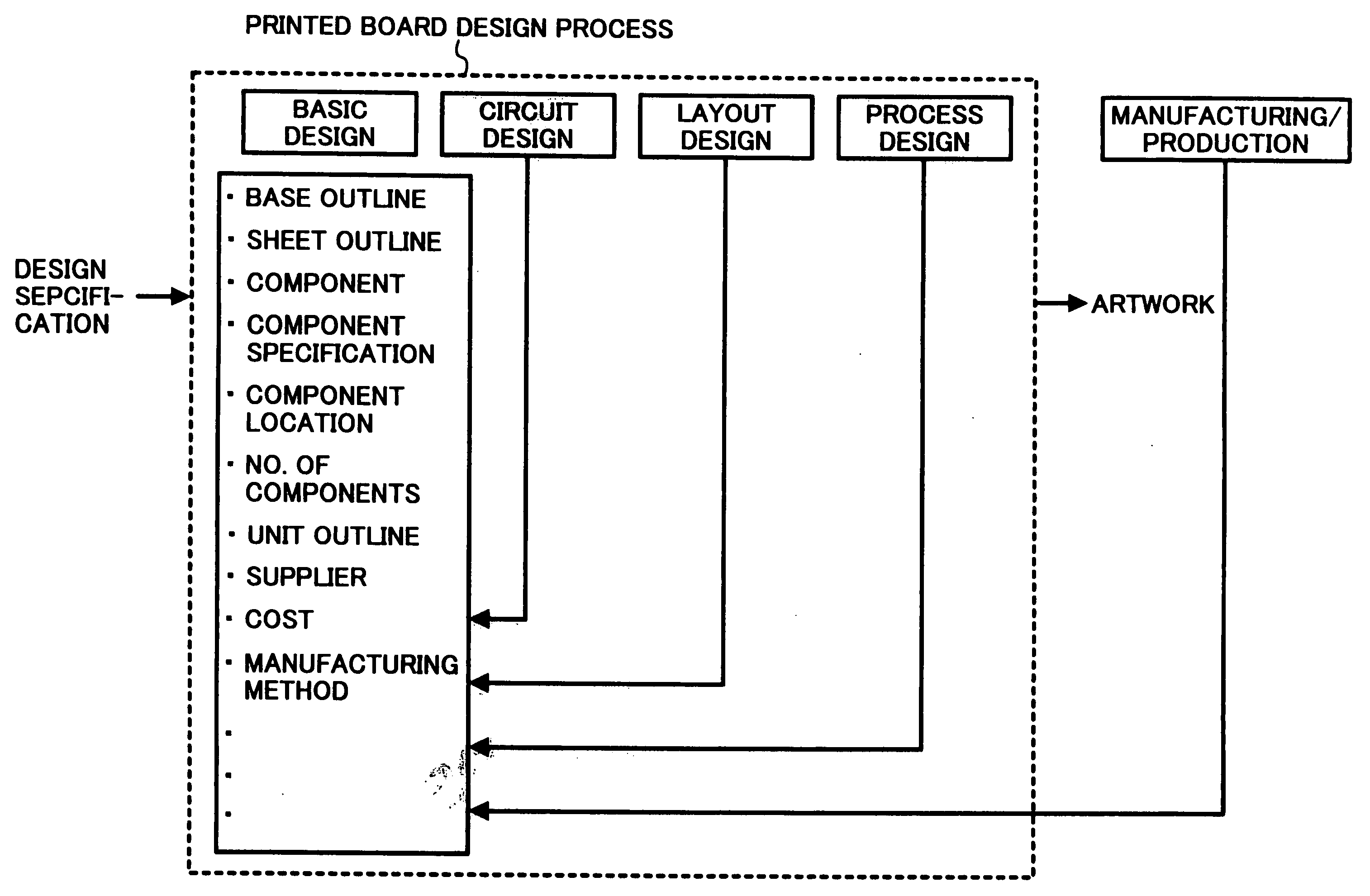
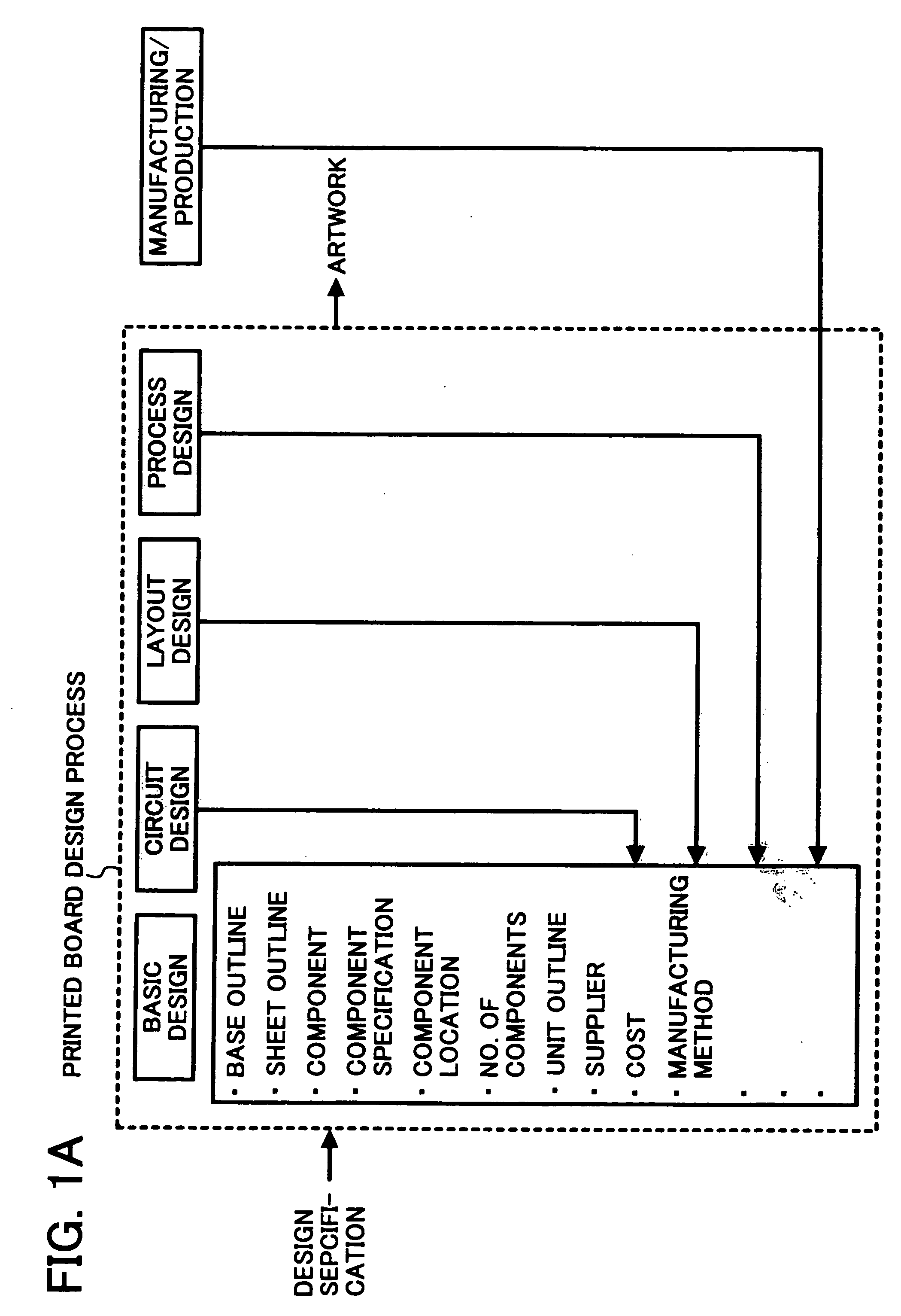
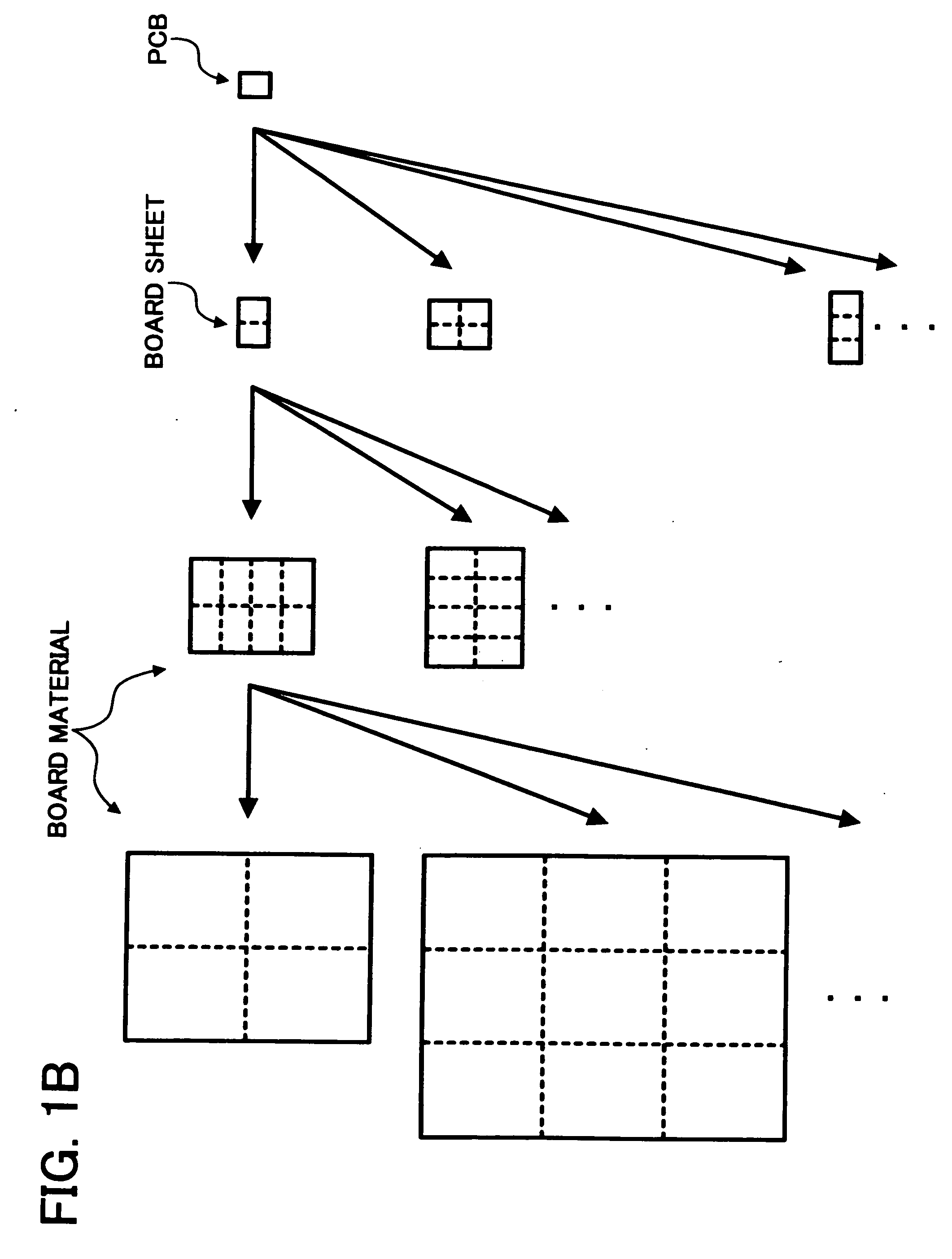
[0020] In describing the exemplary embodiments illustrated in the drawings, specific terminology is employed for clarity. However, the disclosure of this patent specification is not intended to be limited to the specific terminology selected and it is to be understood that each specific element includes all technical equivalents that operate in a similar manner. Referring now to the drawings, wherein like reference numerals designate identical or corresponding parts throughout the several views, FIG. 1A illustrates an exemplary printed board design process, which may be performed before a process of manufacturing or producing a printed circuit board.

[0021] As shown in FIG. 1A, the printed board design process creates the blueprints, such as artwork, to be used for the manufacture / production process based on the PCB design specification. The printed board design process may be performed in several stages including a basic design stage, a circuit design stage, a layout design stage, ...


PUM


Abstract

An apparatus, method, system, computer program and product, each capable of assisting a printed board design process. A predetermined combination including information regarding at least two of a board material, board sheet, and a printed circuit board is prepared before performing the printed board design process.

Description

CROSS REFERENCE TO RELATED APPLICATIONS [0001] This application is related to and claims priority under 35 U.S.C. §119 to Jap. Pat. Appl. No. 2005-079673, filed Mar. 18, 2003, the entire contents of which are hereby incorporated by reference. FIELD OF THE INVENTION [0002] The following disclosure relates generally to an apparatus, method, system, computer program and product, each capable of assisting a printed board design process. DESCRIPTION OF THE RELATED ART [0003] The printed board design process is a process of creating the blueprints, or artwork, for manufacture of a printed circuit board (PCB). As shown in FIG. 1B, one of the most important aspects of the printed board design process is to select a board material or a board sheet that can satisfy the design specification of the PCB (“the PCB design specification”). The selected board material or board sheet is then processed into one or more PCBs during the manufacturing process. For example, the dimensions of the PCB may b...

Claims


Application Information

Patent Timeline
IPC IPC(8): G06F17/50
CPCH05K3/0005G06F17/5068G06F30/39
Inventor HIRAKAWA, HARUNOBUKON, TETSUOTANI, HIDEOISOBE, SHIGERUHIRANO, ATSUSHI
Owner RICOH KK
Why Eureka
Try Eureka