Organic el device and display

a technology of organic el and display, which is applied in the direction of static indicating devices, luminescent compositions, instruments, etc., can solve the problems of insufficient balance of respective luminous intensities of white light emitting organic el devices with the above-mentioned configuration, and it is impossible to obtain a display comparable in color reproduction performance with a crt by using such organic el devices. , to achieve the effect of good balance and excellent balan

Active Publication Date: 2006-10-12
JOLED INC
View PDF8 Cites 70 Cited by
  • Summary
  • Abstract
  • Description
  • Claims
  • Application Information

AI Technical Summary

Benefits of technology

[0014] According to the display as above, by combining a plurality of the organic EL devices excellent in balance between emission

Problems solved by technology

However, the white light emitting organic EL device with the above-mentioned configuration is insufficient in balance of respective luminous intensities in blue, green a

Method used


Image

  • Organic el device and display
  • Organic el device and display
  • Organic el device and display

Examples


example 1

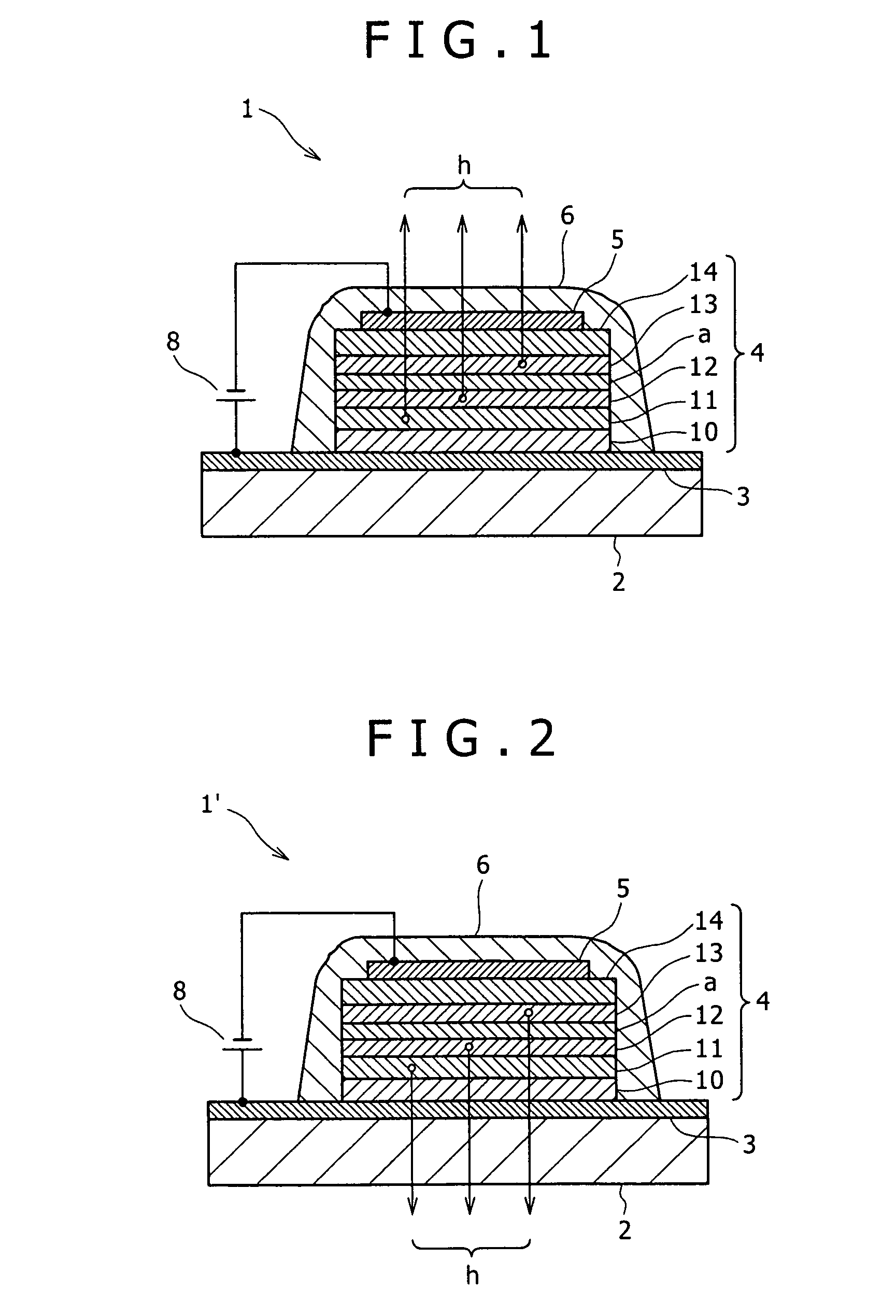
[0081] In Example 1, the bottom emission type organic EL device 1′ described referring to FIG. 2 was manufactured as follows.

[0082] First, a cell for an organic EL device was produced in which a film of ITO (about 100 nm thick) as an anode 3 was formed on a substrate 2 composed of a 30 mm×30 mm glass plate, and other region than a central 2 mm×2 mm light emission region of the anode 3 was masked with an insulation film (omitted in the figure) by use of a photosensitive organic insulation material. Next, a metallic mask having an opening was disposed on the upper side of and in proximity to the substrate 2 in the condition where the opening was matched to the exposed portion of the anode 3 (ITO) to be each light emission region, and the following organic layers were sequentially formed by a vacuum evaporation method under a vacuum of 10-4 Pa or below.

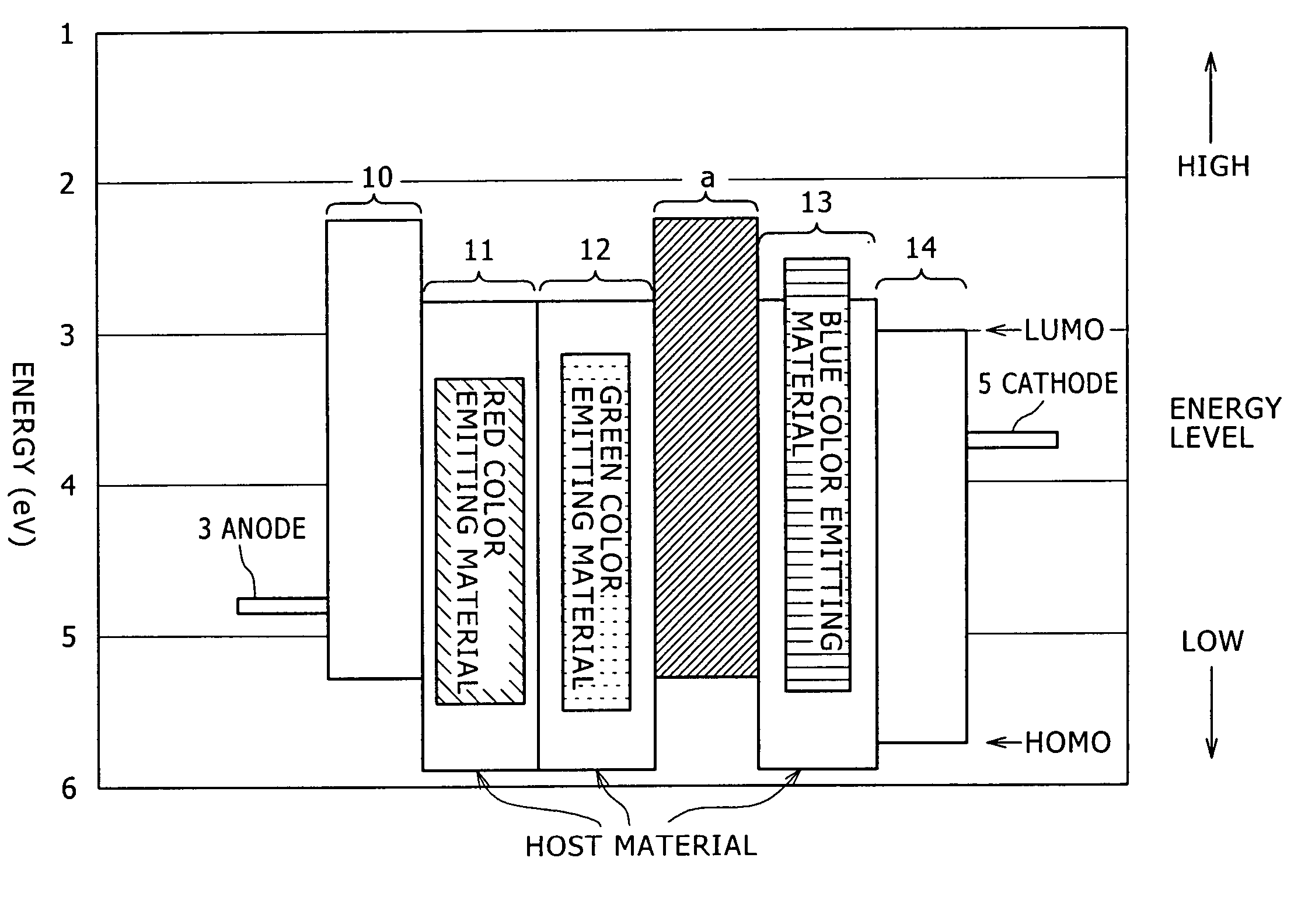
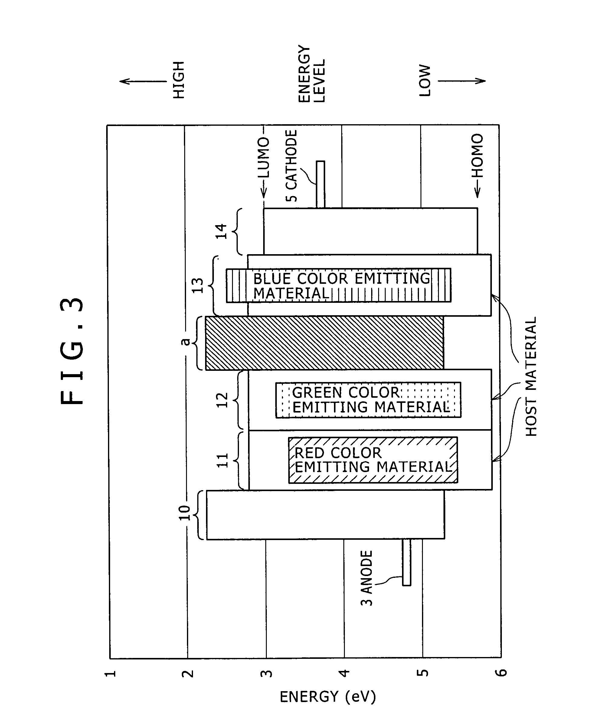
[0083] First, as the hole transport layer 10, a film of m-MTDATA (4,4′, 4″-tris(3-methylphenylphenylamino)-triphenylamine) represente...

example 2

[0091] In Example 2, an organic EL device 1″ of the bottom emission type described referring to FIG. 4 was manufactured. Incidentally, FIG. 6 shows a schematic diagram of the energy level in an organic layer in Example 2.

[0092] In this case, the bottom emission type organic EL device 1″ was manufactured in the same manner as in manufacturing the organic EL device in Example 1 above, except that a step of forming an intermediate layer “a′” between the red light emitting layer 11 and the green light emitting layer 12 was added to the manufacturing procedure in Example 1. It should be noted here, however, that the intermediate layer “a” between the green light emitting layer 12 and the blue light emitting layer 13 was formed in a film thickness of 2 nm (in Example 1, the film thickness was 3 nm). Besides, a film of α-NPD was formed in a thickness of 2 nm as the intermediate layer “a′” between the red light emitting layer 11 and the green light emitting layer 12. The vapor deposition r...


PUM


Abstract

A red light emitting layer 11, a green light emitting layer 12, a blue light emitting layer 13 are laminated in this order between an anode 3 and a cathode 5, and an intermediate layer “a” formed by use of an organic material is provided between the green light emitting layer 12 and the blue light emitting layer 13. The HOMO-LUMO energy gap in the intermediate layer “a” is greater than the HOMO-LUMO energy gap of a green light emitting material constituting the green light emitting layer 12. In addition, the intermediate layer “a” has a hole transporting property. In the case of configuring a display by use of the organic EL devices 1, color filters are provided on the light take-out surface side. This makes it possible to provide an organic EL device with which light emission components for three colors of red, green and blue with a good balance suited to use for a full-color display can be obtained at a high luminance.

Description

TECHNICAL FIELD [0001] The present invention relates to an organic EL device in which an organic layer including a light emitting layer is interposed between an anode and a cathode, and a display using the organic EL device. BACKGROUND ART [0002] In recent years, as a display to be used in place of a cathode ray tube (CRT), flat displays light in weight and low in power consumption have been an object of vigorous research and development. Among the flat displays, those displays which use self-light-emitting type display devices (so-called light emitting devices) such as organic EL (Electroluminescence) devices and organic EL devices have been paid attention to as a display capable of being driven with low power consumption. [0003] Configurations for achieving a full-color display mode with the display using the light emitting devices as above-mentioned include one in which an organic EL device capable of emitting white light is combined with color filters which respectively transmit...

Claims


Application Information

Patent Timeline
IPC IPC(8): G09G3/30C09K11/06H01L51/00H05B33/12H01L51/50H05B33/14H05B33/22H05B33/26
CPCC09K11/06H01L51/5044C09K2211/1011C09K2211/1014C09K2211/186H01L51/005H01L51/0059H01L51/006H01L51/0064H01L51/0071H01L51/0081H01L51/5096H05B33/14H05B33/26C09K2211/1007H10K85/60H10K85/652H10K85/633H10K85/631H10K85/324H10K85/657H10K50/131H10K50/18H05B33/22H05B33/12
Inventor KASHIWABARA, MITSUHIRO
Owner JOLED INC
Why Eureka
Try Eureka