
Electrically responsive device

a technology of responsive devices and electric fields, applied in the direction of photosensitive materials, instruments, specific gravity measurement, etc., can solve the problems of unstable and non-repeatability operating characteristics, wide resonance bands, and non-isolated resonance modes, so as to reduce modal overlap and spillover, improve the resonant response of band passes

Inactive Publication Date: 2006-10-12
BIOSCALE
View PDF22 Cites 55 Cited by
  • Summary
  • Abstract
  • Description
  • Claims
  • Application Information

AI Technical Summary

Benefits of technology

[0013] In one embodiment, correlating excitation and sensing means with the structural property modulation of a device results in an electrical filter (e.g., a surface acoustic wave (SAW) device or a film bulk acoustic resonator (FBAR) device) having a preferred pass band, narrower bandwidth and lower transmission loss than would otherwise be achieved without structural modifications. The pass band includes at least one resonant mode.
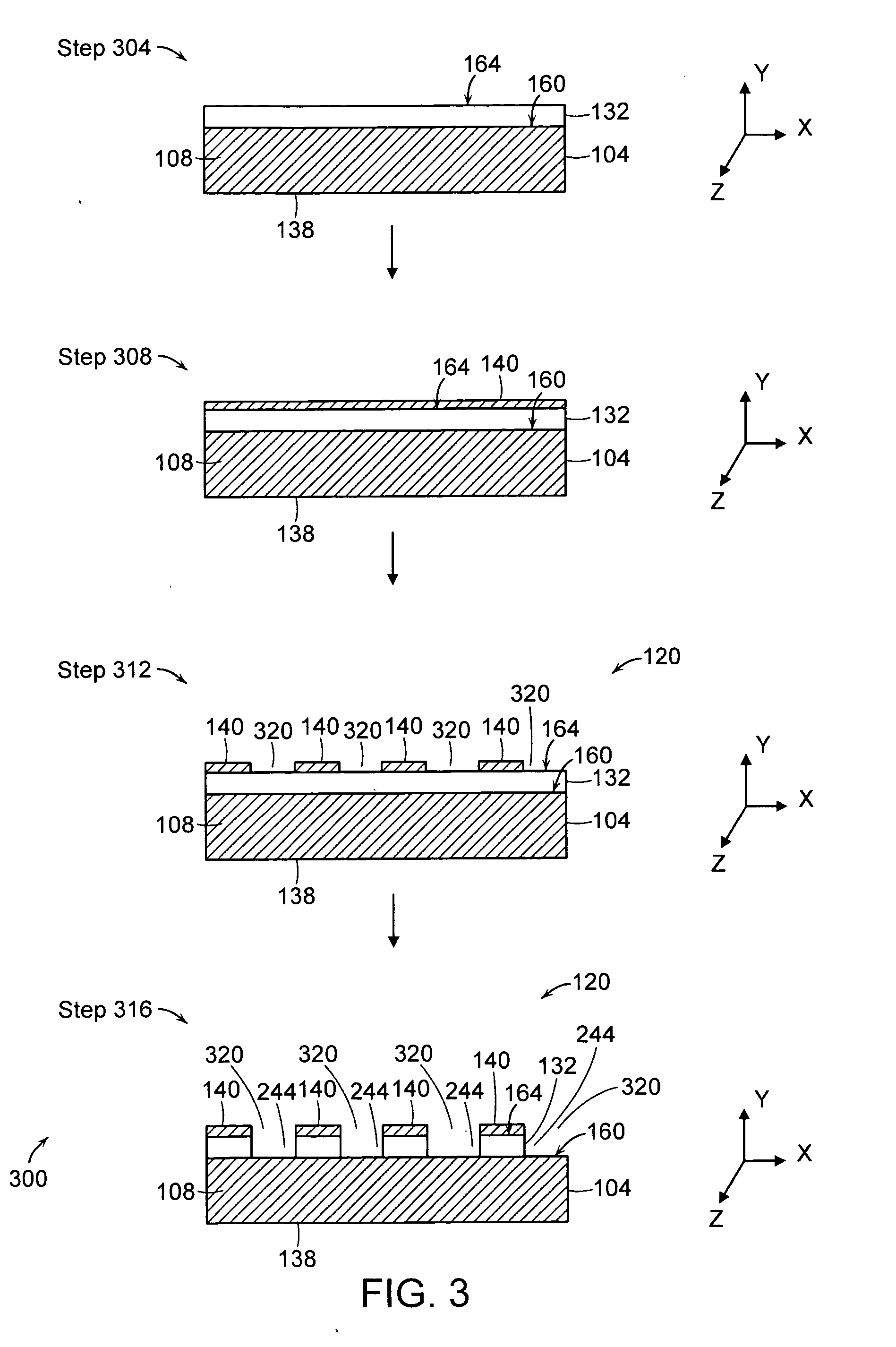
[0018] In some embodiments, the selective removal of the electrode material and the removal of the electrically responsive material substantially improves the band pass resonant response (e.g., modes greater than the first mode) of the device.
[0019] In some embodiments, the invention relates to a method for modifying a resonance mode of the response of the device by enforcing that resonance mode of response of the device. In some embodiments, a particular pattern of the electrode material is used to enforce a resonance mode of response of the device. In some embodiments, removal of the electrically responsive material substantially modifies at least one resonance mode of response of the device by reducing modal overlap and spillover associated with other resonance modes of the device.
[0030] The invention, in another aspect, features an electrically responsive device that includes a substrate material and at least one electrically responsive element on the substrate. The device also includes an electrode material on a surface of the at least one electrically responsive element, wherein the electrically responsive element and the electrode material are patterned on the substrate layer to modify at least one resonance mode of response of the device by reducing modal overlap and spillover associated with other resonance modes of the device.
[0045] The invention, in another aspect, features an electrically responsive device including a composite structure having spatially modulated properties. The device also includes means of exciting and sensing motion of the structure that is substantially correlated with the spatially modulated properties to produce a narrow (e.g., with respect to frequency) and low loss (e.g., having a more pronounced transfer function peak) pass band. Advantages according to the invention can be achieved in devices exposed to fluid loading or in devices not exposed to fluid loading.

Problems solved by technology

Variations in the devices (e.g., due to manufacturing tolerances) tend to result in non-isolated resonance modes, wide resonance bands, high loss, and unstable and non-repeatable operating characteristics.

Method used


Image

  • Electrically responsive device
  • Electrically responsive device
  • Electrically responsive device

Examples


Embodiment Construction

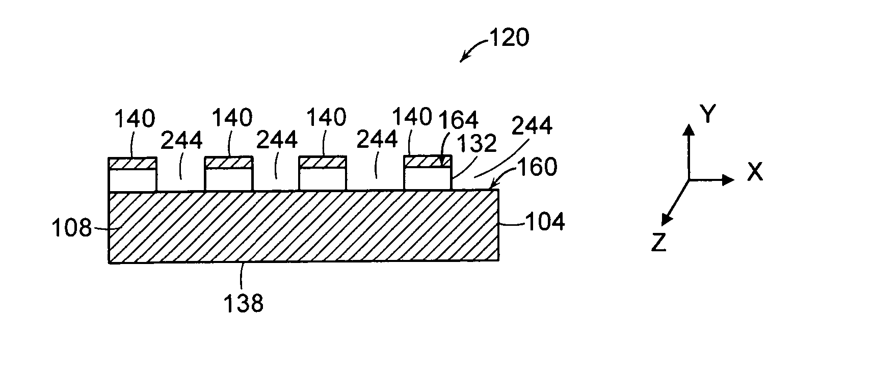
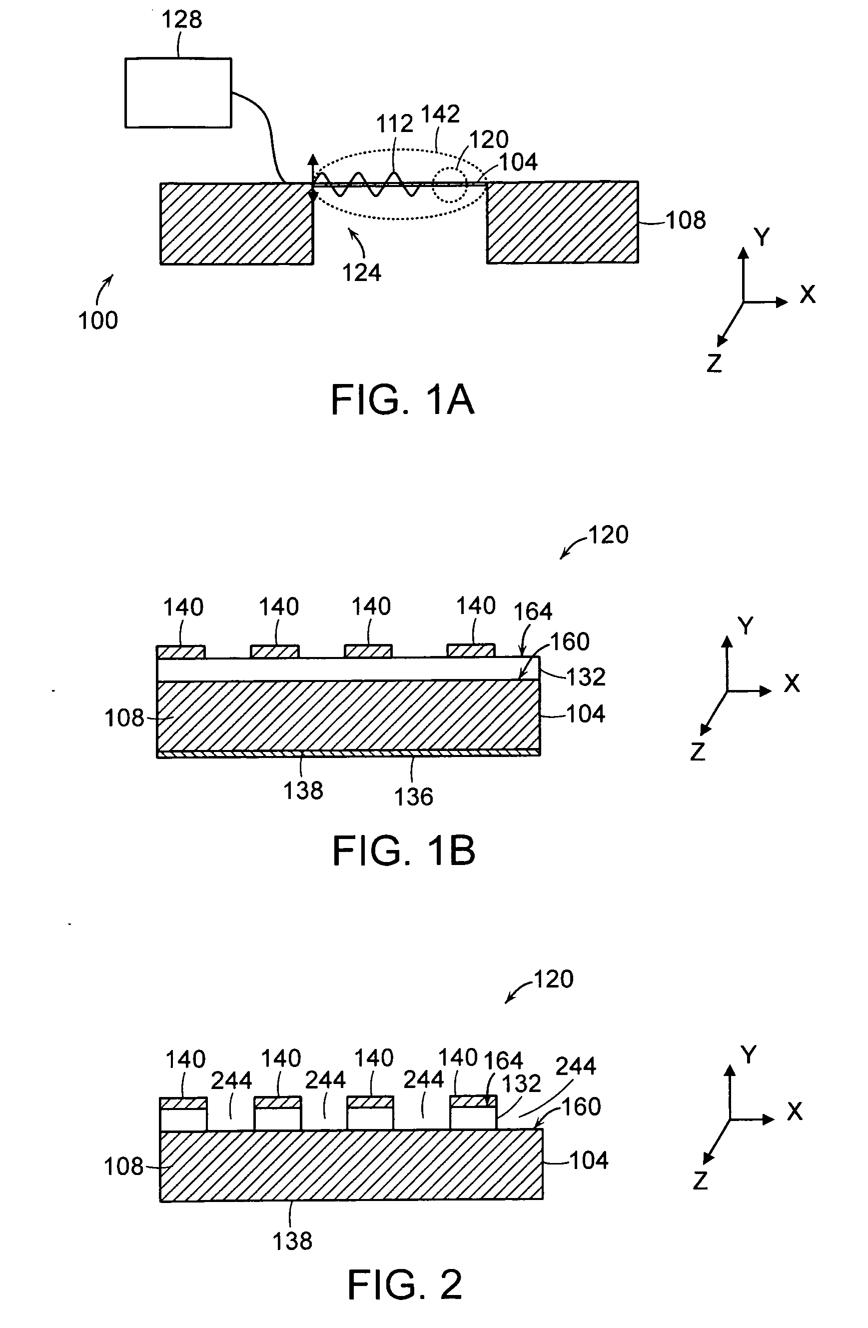
[0058]FIG. 1A is a schematic illustration of an electrically responsive device 100. In this embodiment, the electrically responsive device 100 is a resonant device constructed from a substrate 108 (e.g., a silicon wafer) using micro-fabrication techniques known in the art. Alternative methods of fabrication are possible without departing from the scope of the present invention. In this embodiment, a cavity 124 is etched into the substrate 108 to produce a thin, suspended membrane 104 that is approximately 1.6 mm long (along the X-Axis), 0.3 mm wide (along the Z-Axis) and 2 μm thick (along the Y-Axis). The overall substrate 108 thickness is approximiately 500 μm, so the depth of the cavity 124 is just slightly less than the substrate 108 thickness. A 0.5 μm layer of an electrically responsive material 132 (e.g., an electroactive or electrooptical material) is deposited over an outer surface 160 (i.e., the surface opposite the cavity 124) of the membrane 104, as shown in a region 120 ...


PUM


Abstract

Electrically responsive devices and methods for fabricating electrically responsive devices involves applying an electrically responsive material (e.g., an electroactive material) over at least a portion of a surface of a substrate material and applying an electrode material over at least a portion of a surface of the electrically responsive material. At least one region of the electrode material is selectively removed exposing the electrically responsive material. At least some of the electrically responsive material is selectively removed in a region corresponding to the at least one region of the electrode material.

Description

RELATED APPLICATIONS [0001] This application claims priority to U.S. provisional application Ser. No. 60 / 668,933, filed on Apr. 6, 2005, and entitled “Micromachined Electroactive Resonant Device,” the entirety of which is hereby incorporated herein by reference.FIELD OF THE INVENTION [0002] The present invention generally relates to electrically responsive devices and methods for fabricating electrically responsive devices. BACKGROUND OF THE INVENTION [0003] Electrically responsive devices are those devices that generate an output signal in response to an electrical signal and / or generate an electrical signal in response to an input signal. Typical types of input and output signals include electrical, optical, electromagnetic, vibrational, and thermal signals. One type of electrically responsive devices is a resonant device. [0004] Resonant devices, such as surface acoustic wave devices, bulk acoustic wave devices, flexural plate / lamb wave devices, and quartz crystal microbalance de...

Claims


Application Information

Patent Timeline
IPC IPC(8): G01T1/00
CPCG01N9/002G01N2291/0256G01N29/036H03H3/00H03H3/10H03H3/04
Inventor MASTERS, BRETT P.MILLER, MICHAEL F.
Owner BIOSCALE
Learn More