Electronic circuit, method of driving electronic circuit, electro-optical device, and electronic apparatus

a technology of electronic circuits and light-emitting elements, applied in static indicating devices, instruments, material analysis, etc., can solve the problems of the variation of the pd of each pixel circuit b>17/b>

Active Publication Date: 2006-10-19
ELEMENT CAPITAL COMMERCIAL CO PTE LTD
View PDF1 Cites 127 Cited by
  • Summary
  • Abstract
  • Description
  • Claims
  • Application Information

AI Technical Summary

Benefits of technology

[0013] An advantage of some aspects of the invention is that it provides an electronic circuit which is capable of preventing a gray-scale level of each light-emitting element from varying due to the voltage drop in a power supply line, a method of driving an electronic circuit, an electro-optical device, and an electronic apparatus.

Problems solved by technology

Accordingly, the potentials VH supplied to the respective pixel circuits P0 are different from each other while depending on the corresponding locations of the respective pixel circuits P. In addition, there is a problem in that a gray-scale level of a light-emitting element 17 of each pixel circuit PD may vary due to the difference between the potentials VH.

Method used


Image

  • Electronic circuit, method of driving electronic circuit, electro-optical device, and electronic apparatus
  • Electronic circuit, method of driving electronic circuit, electro-optical device, and electronic apparatus
  • Electronic circuit, method of driving electronic circuit, electro-optical device, and electronic apparatus

Examples


first embodiment

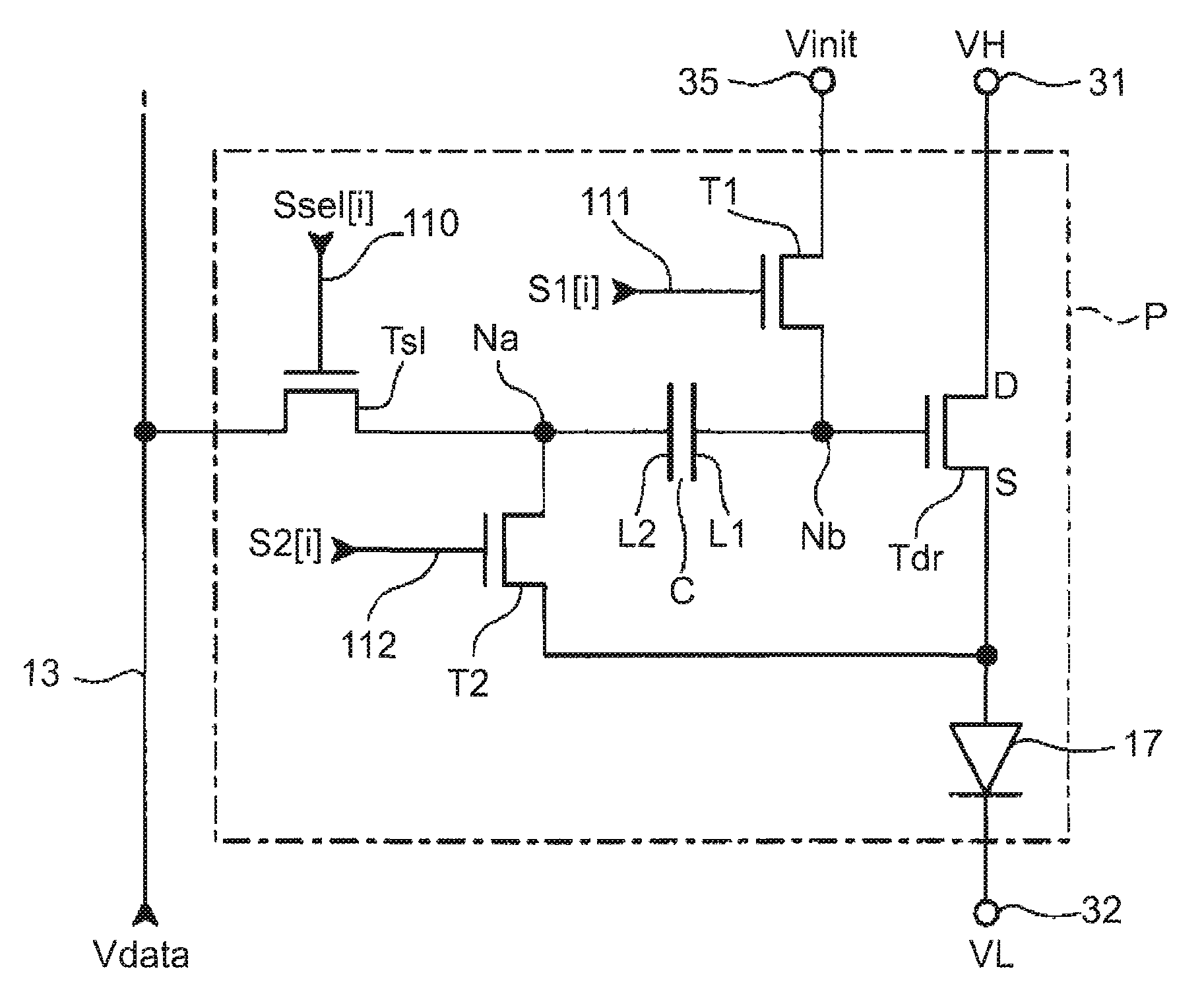
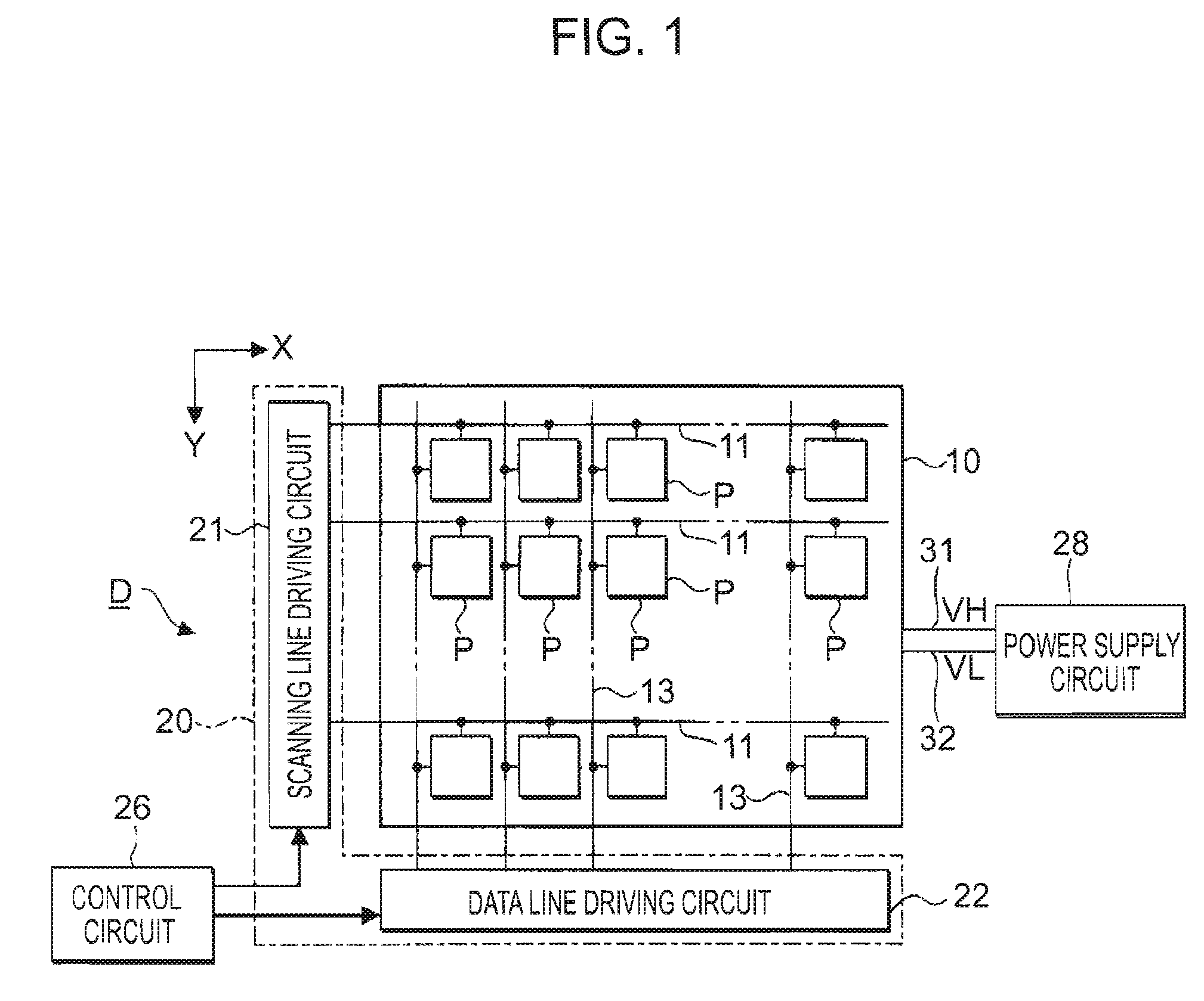
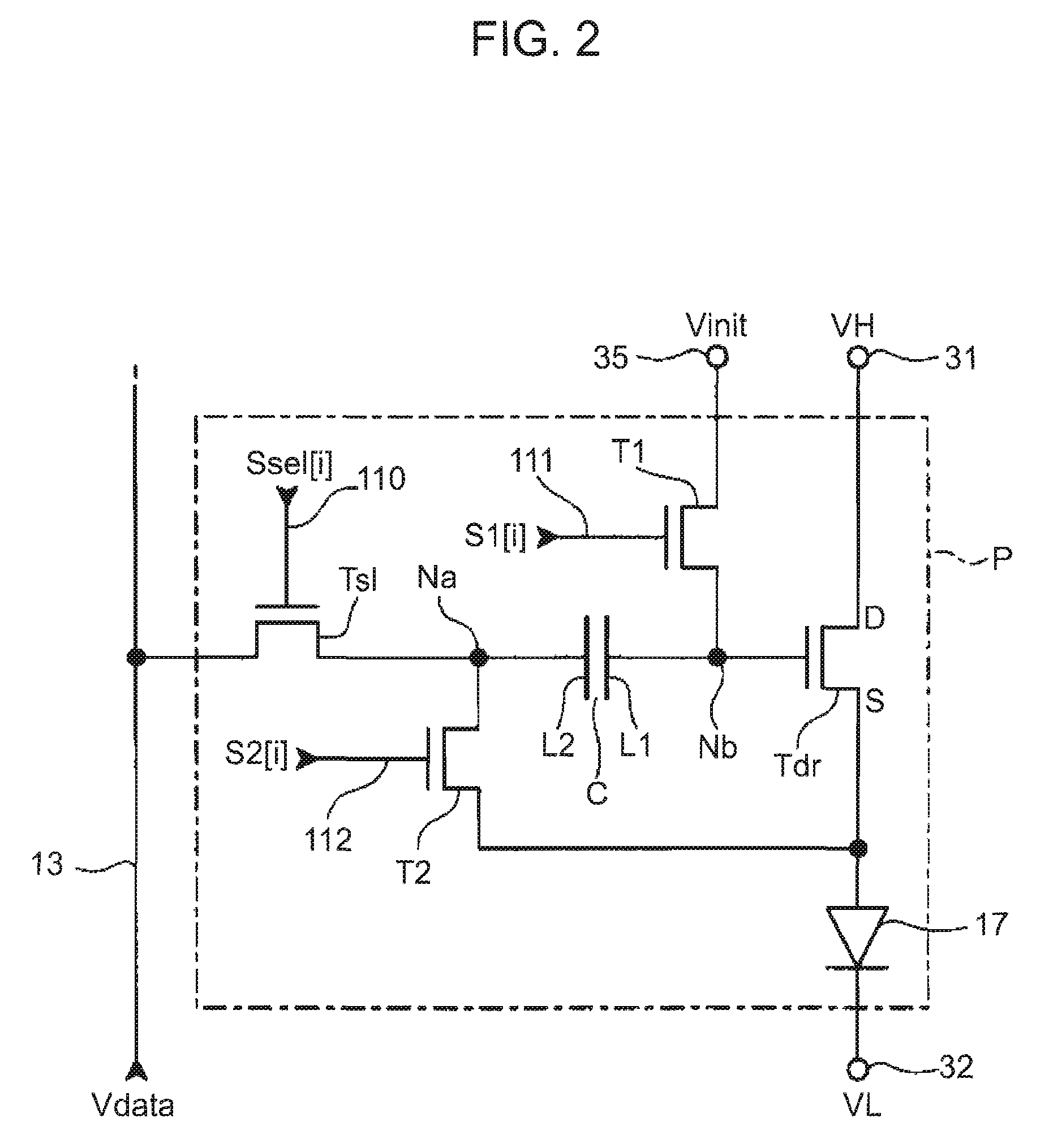
[0056]FIG. 1 is a block diagram illustrating a structure of an electro-optical device according to a first embodiment of the invention. An electro-optical device D (serving as an image display unit) is used in various electronic apparatuses. Specifically, the electro-optical device D includes a substrate 10 on which a plurality of pixel circuits P are disposed, a driving circuit 20 that drives the respective pixel circuits P, a control circuit 26 that controls the operation of the driving circuit 20, and a power supply circuit 28 that supplies a power to the respective units. All or a part of each of the driving circuit 20, the control circuit 26, and the power supply circuit 28 is mounted on a wiring board (not shown) that is bonded to the substrate 10. However, an IC chip, on which these circuits are mounted, may be mounted on the surface of the substrate 10 or these circuits may be mounted by means of thin film transistors that are formed on the surface of the substrate 10.

[0057...

second embodiment

[0080] Next, a second embodiment of the invention will be described.

[0081] In the first embodiment, each of the scanning signal Ssel [i], the first control signal S1[i], and the second control signal S2 [i] is constructed as an individual signal, but at least one of these signals may serve as another signal. In the pixel circuit P in the second embodiment, the scanning signal Ssel [i] serves as the first control signal S1[i] (that is, the first control signal S1 [i] serves as the scanning signal Ssel [i]). In addition, constituent elements of the other embodiments (which will be described in detail below), which are the same as those of the first embodiment, are denoted by the same reference numerals, and the description thereof will be properly omitted.

[0082]FIG. 5 is a circuit diagram illustrating a structure of a pixel circuit P according to the present embodiment. As shown in FIG. 5, in the pixel circuit P according to the present embodiment, the gate terminal of the first swi...

third embodiment

[0085] Next, a third embodiment of the invention will be described. In the first embodiment, separately from the scanning signal Ssel[i], the first control signal S1[i], and the second control signal S2[i], the initialization potential Vinit is generated by the power supply circuit 28, but the signal, which is generated by the scanning line driving circuit 21, may be used as the initialization potential Vinit. In the present embodiment, the pixel circuit P may be constructed such that the second control signal S2[i] is also used as the initialization potential Vinit.

[0086]FIG. 8 is a circuit diagram illustrating a structure of the pixel circuit P according to the present embodiment. As shown in FIG. 8, in the present embodiment, the drain terminal of the first switching element T1 and the gate terminal of the second switching element T2 are connected to the second control line 112. That is, the second control signal S2[i], which is output from the scanning line driving circuit 21, ...


PUM


Abstract

There is provided a method of driving an electronic circuit. The electronic circuit includes a light-emitting element that is interposed between a first electric supply line and a second electric supply line having different potentials and emits light by the supply of a current, a storage capacitor that holds a voltage between a first electrode and a second electrode, and a driving transistor that is interposed between the first electric supply line and the second electric supply line and has a gate terminal connected to the first electrode of the storage capacitor. The method includes: for a first period, applying a data potential according to a gray-scale level designated for the light-emitting element to the second electrode of the storage capacitor while electrically connecting an initialization wiring line supplied with an initialization potential to the first electrode of the storage capacitor; and for a second period subsequent to the first period, electrically connecting the second electrode of the storage capacitor to a source terminal of the driving transistor.

Description

BACKGROUND [0001] 1. Technical Field [0002] The present invention relates to a technology for controlling behavior of a light-emitting element, such as an organic light-emitting diode element (hereinafter, referred to as ‘OLED’ element) or the like. [0003] 2. Related Art [0004] In general, electro-optical devices, in which a light-emitting element, such as an OLED element or the like, is used, have been suggested as display devices of various electronic apparatuses. This kind of electro-optical device has a structure in which a plurality of pixel circuits, each of which has a light-emitting element, are disposed in a matrix. Each of the pixel circuits controls a current supplied to the light-emitting element. [0005]FIG. 28 is a circuit diagram illustrating a structure of one pixel circuit in an electro-optical device according to the related art (for example, see ‘2001FPD Technology Outlook’, Electronic Journal, p 749 to 750). As [0006] shown in FIG. 28, a pixel circuit P0 includes ...

Claims


Application Information

Patent Timeline
Patent Type & Authority Applications(United States)
IPC IPC(8): H01L31/00H05B44/00
CPCG09G3/3233G09G2320/0223G09G3/3291G09G3/30G09G3/20
Inventor KASAI, TOSHIYUKI
Owner ELEMENT CAPITAL COMMERCIAL CO PTE LTD
Why Eureka
Try Eureka