Semiconductor device

Active Publication Date: 2006-10-19
LAPIS SEMICON CO LTD
View PDF8 Cites 4 Cited by
  • Summary
  • Abstract
  • Description
  • Claims
  • Application Information

AI Technical Summary

Benefits of technology

[0008] It is therefore an object of the present invention to resolve the above-described problems and to provide a semiconductor device which has improved sealing characteristics, and which is therefore capable of preventing moisture from entering through gaps formed between each side of a conductive post and the sealing resin and thus improve its moisture resistance ability, and capable of preventing the conductive post from being displaced due to external force and thus improve its mechanical strength.
[0010] In accordance with a second aspect of the present invention, a method of manufacturing a semiconductor device comprises the steps of: preparing a semiconductor substrate having an electrode pad on the surface; forming a wiring above the semiconductor substrate, the wiring electrically connecting with the electrode pad; forming a conductive post on the wiring, the conductive post electrically connecting with the wiring; forming a sealing resin over the semiconductor substrate and the wiring, the height of the upper face of the sealing resin being approximately the same as the height of the upper surface of the conductive post, and the sealing resin and the conductive post having a gap formed between them; forming an external electrode on the conductive post, the external electrode electrically connecting with the conductive post; filling a liquid material into the gap between the sealing resin and the conductive post, the liquid material having thermosetting and insulation properties; and forming an insulator on the lateral surfaces of the conductive post by causing the liquid material to harden by means of a thermal treatment.

Problems solved by technology

However, the adhesiveness between the sealing resin and the conductive posts is not necessarily sufficient.
When the adhesiveness between the sealing resin and the conductive posts becomes weak due to manufacturing error etc., the sealing resin may become easily separated from the lateral surfaces of the conductive posts, which results in the generation of gaps between the sealing resin and the conductive posts.
When gaps are generated between the sealing resin and the conductive posts, there is a possibility, for instance, that moisture will enter inside the package through the gaps, which may result in the occurrence of corrosion on the elements made of a metal material, such as the conductive posts and the wirings.
As for other possible problems which may be caused by having gaps between the sealing resin and the conductive posts, for instance, the conductive posts may be displaced due to external force, which may result in the generation of cracks in the insulation film etc. on the surface of the semiconductor chip.
However, forming a copper oxide film on the lateral surfaces of the columnar electrodes requires a large number of processes, such as a wet-etching process for making the surfaces of the columnar electrodes pure copper surfaces, a pre-baking process for making the substrate temperature uniform at a predetermined temperature, a main baking process for oxidizing the surfaces of the columnar electrodes in order to form the copper oxide film, and so forth.
Such increase in the number of processes inevitably leads to an increase in production costs.

Method used


Image

  • Semiconductor device
  • Semiconductor device
  • Semiconductor device

Examples


first embodiment

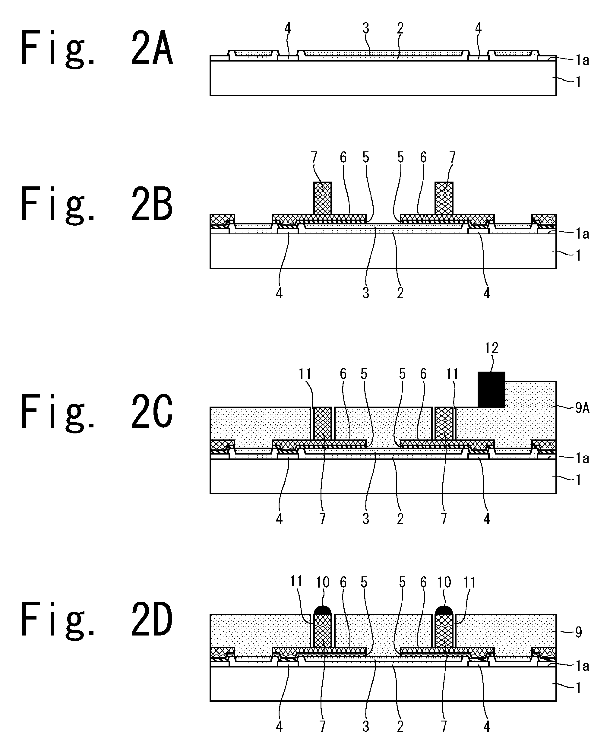
[0022] First, a first embodiment of the present invention will be described in detail with reference to the drawings.

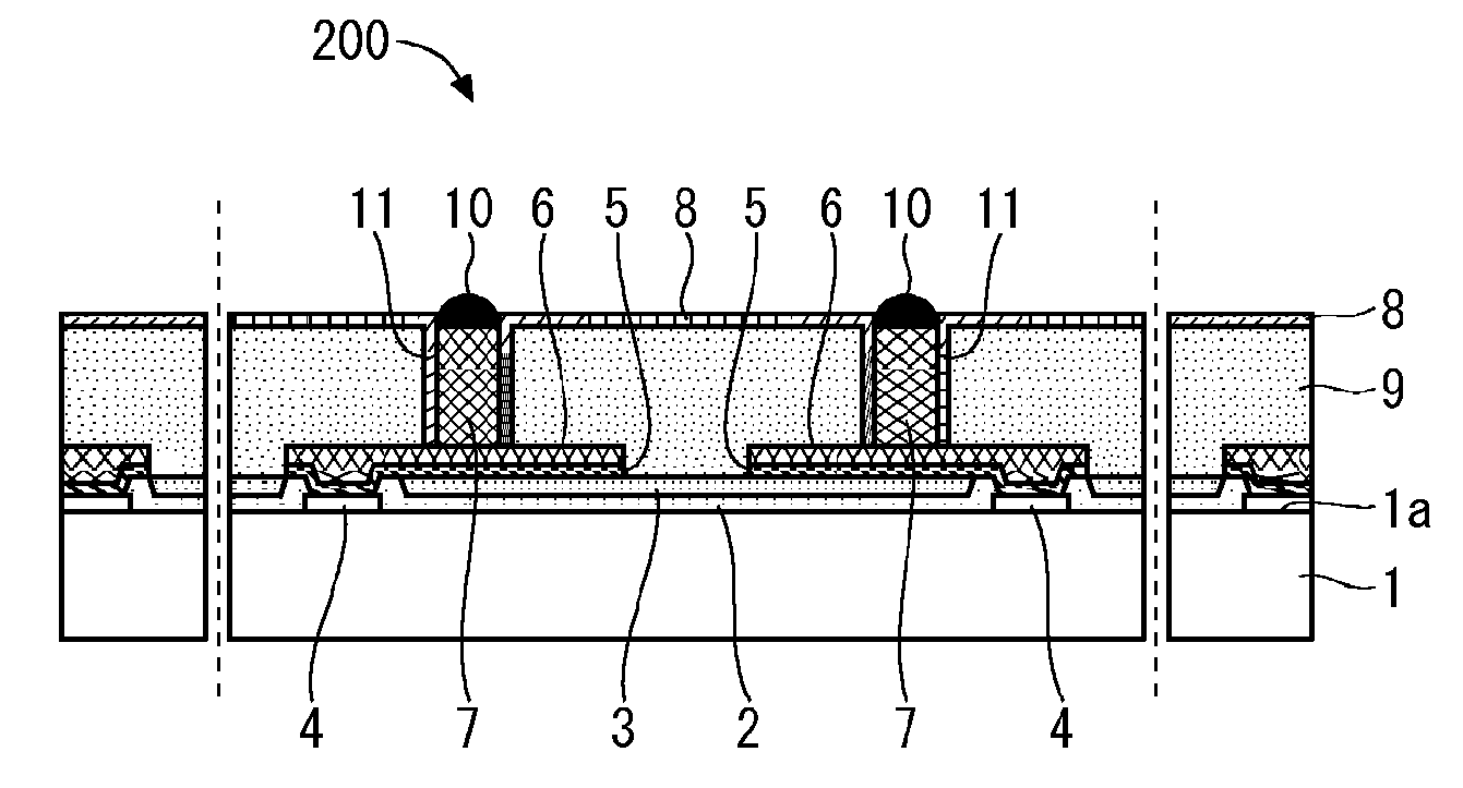
[0023]FIG. 1 is a diagram showing a cross sectional view of a portion of a semiconductor device 100 according to the first embodiment of the present invention. The semiconductor device 100 is a resin-sealed type semiconductor device manufactured by using a W-CSP technique, and includes a semiconductor substrate 1, protective films 2 and 3, electrode pads 4 (only one electrode pad 4 is shown in FIG. 1), conducting films 5 (only a portion of the conducting film 5 is shown in FIG. 1), wirings (also called re-wirings) 6 (only a portion of the wirings 6 are shown in FIG. 1), conductive posts 7 (only one conductive post 7 is shown in FIG. 1), an insulation film 8, a sealing resin 9, and external electrodes 10 (only one external electrode 10 is shown in FIG. 1).

[0024] The semiconductor substrate 1 has an electronic circuit (not shown) configured with one or more semiconduc...

second embodiment

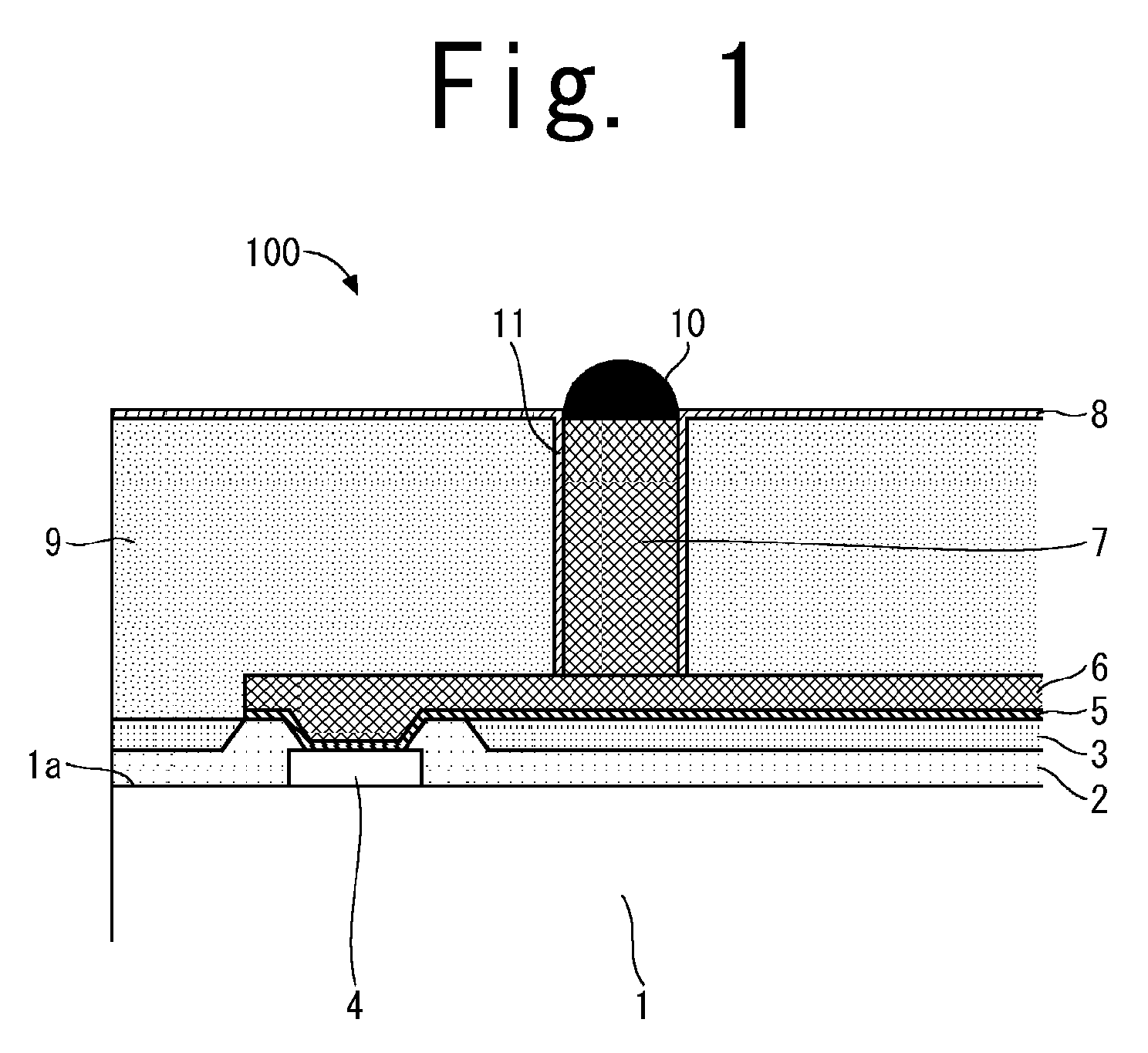
[0047] Next, a second embodiment of the present invention will be described in detail with reference to the drawings. FIG. 4 is a diagram showing a cross sectional view of a portion of a semiconductor device 200 according to the second embodiment of the present invention.

[0048] The semiconductor device 200 is a resin-sealed type semiconductor device manufactured by using a W-CSP technique, and it has the same structure as the semiconductor device 100 of the first embodiment (shown in FIG. 1), except that the insulation film 8 for filling the gaps 11 generated between the conductive posts 7 and the sealing resin 9 is replaced with insulation films 8a.

[0049] Since the rest of the structure is the same as the structure of the semiconductor device 100 of the first embodiment, the same reference numbers will be used for the structural elements that are the same as the first embodiment, and redundant explanation of those structure elements will be omitted.

[0050] The insulation films 8a...


PUM


Abstract

A semiconductor device includes a semiconductor substrate, an electrode pad, a wiring, a conductive post, an insulator, a sealing resin, and an external electrode. The electrode pad is formed on the main surface of the semiconductor substrate. The wiring is formed above the semiconductor substrate, the wiring electrically connecting with the electrode pad. The conductive post is formed on the upper surface of the wiring, the conductive post electrically connecting with the wiring. The insulator is formed on the lateral surfaces of the conductive post and has a thermosetting property. The sealing resin is formed over the semiconductor substrate and the wiring and on the surface of the insulator. The external electrode is formed on the conductive post, the external electrode electrically connecting with the conductive post.

Description

BACKGROUND OF THE INVENTION Field of the Invention [0001] The present invention relates to a semiconductor device, particularly to a chip-size packaged resin-sealed type semiconductor device. Moreover, the present invention also relates to a method of manufacturing such semiconductor device. Background Information [0002] In recent years, as portable devices typified by notebook PCs and cellular phones become rapidly popular, semiconductor devices to be mounted on such portable devices must become smaller, thinner and lighter. One key technology which realizes such needs is a high-density packaging technique, such as a CSP (chip size package) which is extremely close to the size of a semiconductor chip. Particularly, a W-CSP (Wafer Level Chip Size Package) technique, in which the sealing process is done in a wafer state, is considered to be an ultimate compact package, and it is drawing increasing attention because may provide advantages such as reduction in manufacturing costs. [000...

Claims


Application Information

Patent Timeline
IPC IPC(8): H01L23/48
CPCH01L21/561H01L23/3114H01L24/13H01L24/10H01L2224/13099H01L2924/01013H01L2924/01022H01L2924/01029H01L2924/01057H01L2924/01074H01L2924/01075H01L2924/01078H01L2924/01005H01L2924/01006H01L2924/01033H01L2924/014H01L2924/00H01L2224/05569H01L2224/05024H01L2224/05008H01L2224/05022H01L2224/05001H01L2224/05124H01L2224/05147H01L2224/05166H01L2224/056H01L2224/1191H01L2224/1184H01L24/05H01L2224/02377H01L2224/131H01L2224/13H01L2924/00014
Inventor NAGASAKI, KENJI
Owner LAPIS SEMICON CO LTD
Why Eureka
Try Eureka