Heat dissipating structure for IC chip of plasma display module and plasma display module having the same

a technology of ic chip and plasma display module, which is applied in the direction of television system, identification means, instruments, etc., can solve the problems of reducing the performance and lifespan reducing the heat dissipation efficiency so as to improve the heat dissipation performance of the ic chip and prevent contamination

Inactive Publication Date: 2006-11-02
SAMSUNG SDI CO LTD
View PDF18 Cites 13 Cited by
  • Summary
  • Abstract
  • Description
  • Claims
  • Application Information

AI Technical Summary

Benefits of technology

[0009] It is therefore an object of the present invention to provide an improved design for a plasma display module.
[0010] It is also an object of the present invention to provide an improved heat dissipating structure for a plasma display module.
[0011] It is further an object of the present invention to provide an improved heat dissipating structure for an IC chip located on a signal transmitting member that delivers signals that drives a plasma display panel in a plasma display module.
[0013] It is yet an object of the present invention to provide a heat dissipating structure for an integrated circuit (IC) chip of a plasma display module, and a plasma display module having the same, that can improve the heat dissipating performance of the IC chip while preventing contamination by a chip heat-dissipating sheet by installing a thermally conductive member covering the chip heat-dissipating sheet.

Problems solved by technology

When the plasma display panel is driven, the IC chip generates a lot of heat.
A conventional heat dissipating structure for the IC chip cannot effectively dissipate this heat, leading to a reduction in performance and lifespan of the IC chip.
However, such materials can also be apt to generate foreign material.
If this foreign material spreads throughout the plasma display device, many problems can occur, such as short circuiting.

Method used


Image

  • Heat dissipating structure for IC chip of plasma display module and plasma display module having the same
  • Heat dissipating structure for IC chip of plasma display module and plasma display module having the same
  • Heat dissipating structure for IC chip of plasma display module and plasma display module having the same

Examples


first embodiment

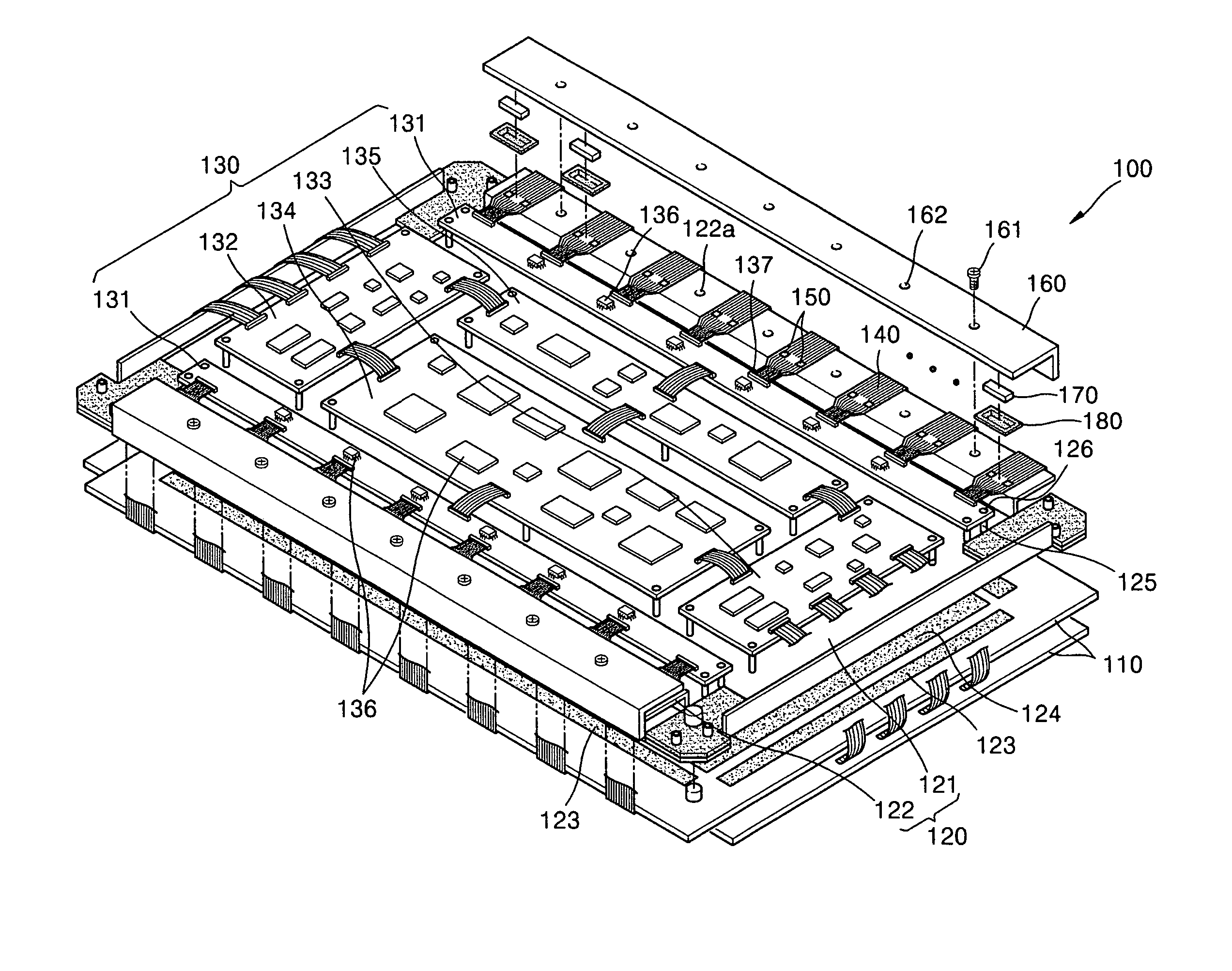
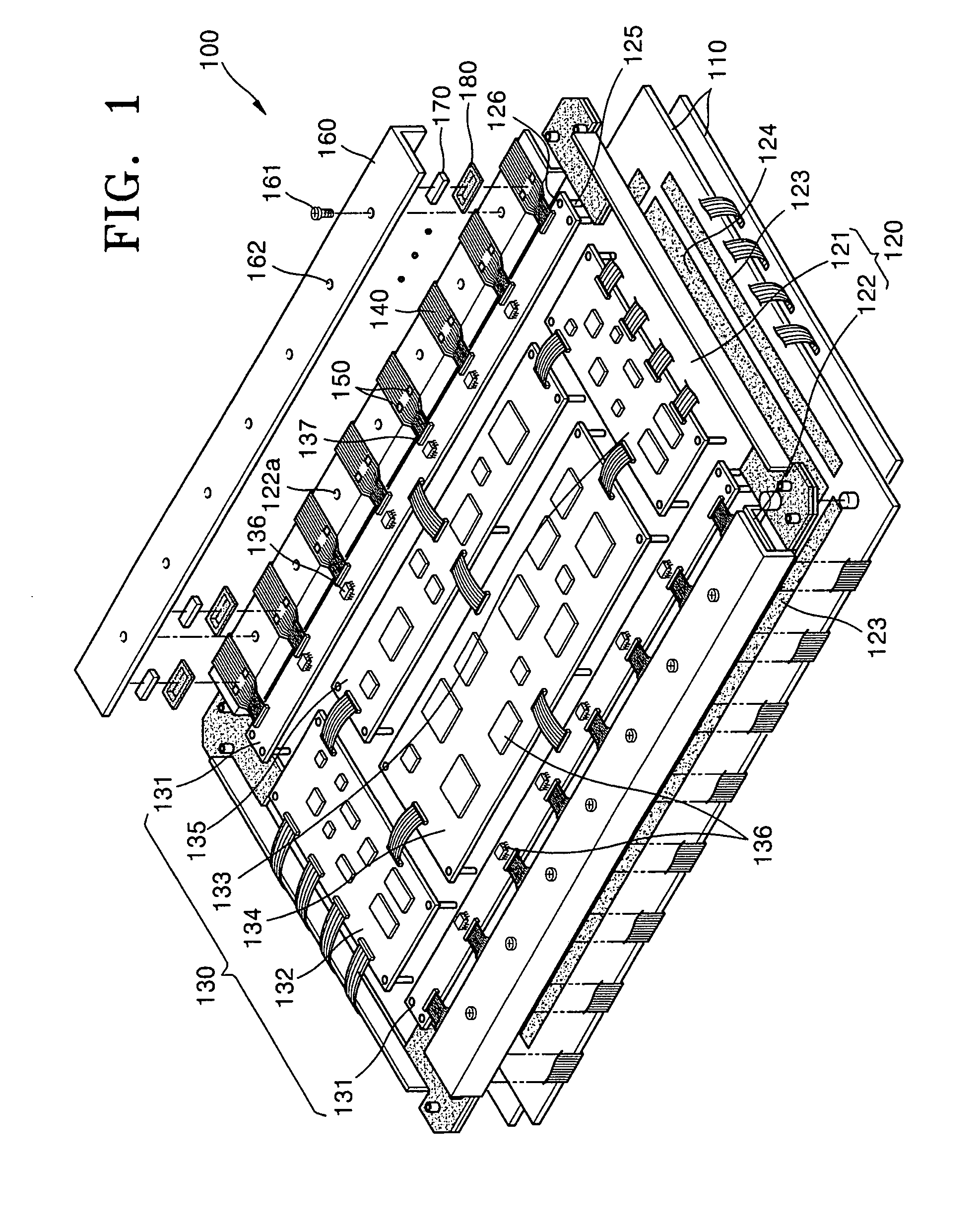
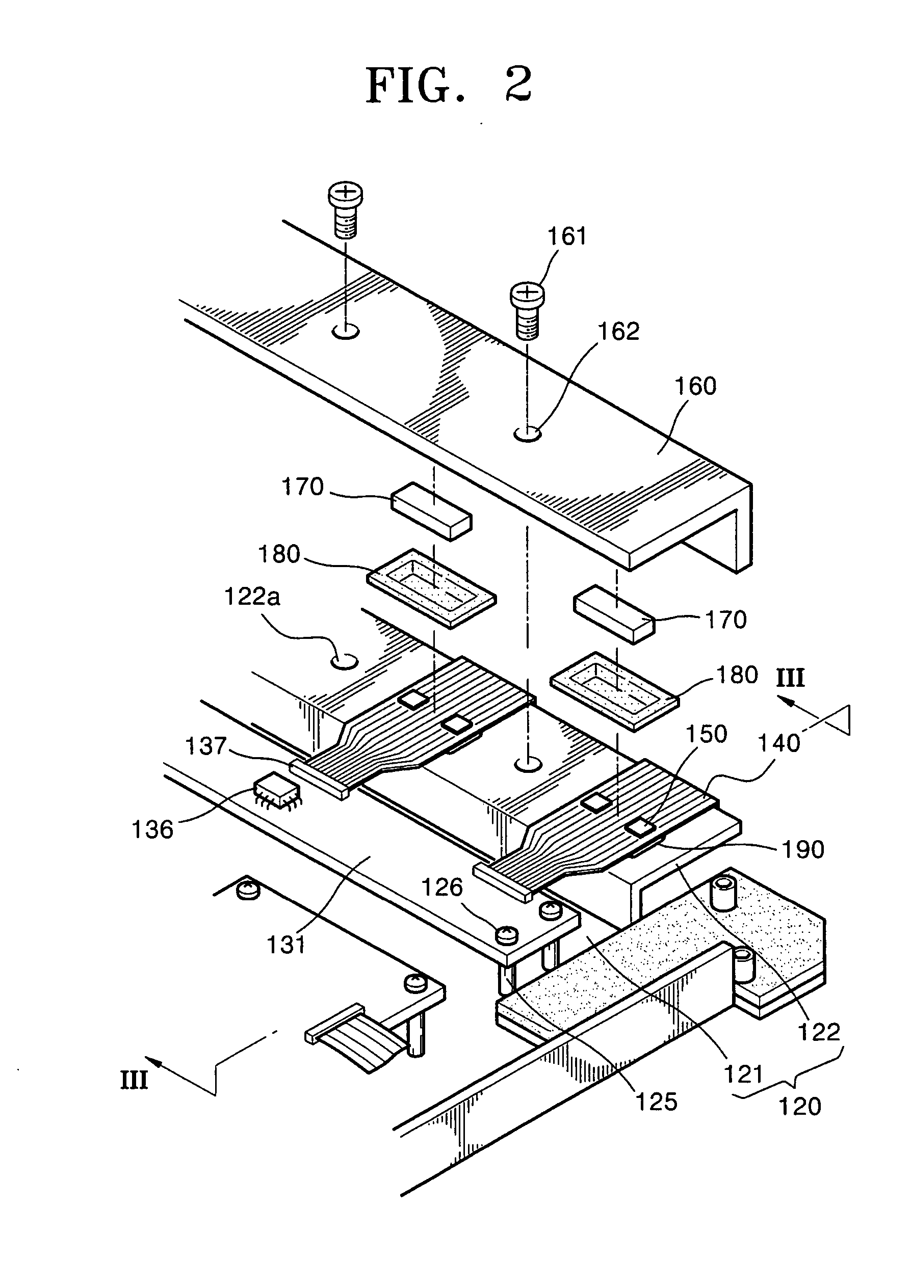
[0033] Turning now to FIGS. 1 through 3, FIG. 1 is an exploded perspective view of a plasma display module 100 having a heat dissipating structure for an IC chip according to the present invention, FIG. 2 is an exploded perspective view of a portion of the chassis bending part 122 of the plasma display module 100 of FIG. 1, and FIG. 3 is a magnified cross-sectional view of the chassis bending part 122 of FIG. 2 taken along line III-III. As shown in FIG. 1, the plasma display module 100 includes a plasma display panel 110, a chassis 120, circuit boards 130, a signal transmitting member 140, an integrated circuit (IC) chip 150, a cover plate 160, a chip heat-dissipating sheet 170, and a thermally conductive member 180.

[0034] The plasma display panel 110 is mounted on the front surface of the chassis 120, using a double-sided adhesive means 123 such as double sided tape attached to the rear surface of the plasma display panel 110. A panel heat-dissipating sheet 124 made of a material h...

second embodiment

[0056] In the second embodiment, the circuit boards 230 include address electrode buffer circuit boards 231, an X electrode driving circuit board 232, a Y electrode driving circuit board 233, a power supply board 234, and a logic control board 235. Each of the circuit boards 230 include a plurality of circuit elements 236. The circuit boards 231, 232, 233, 234 and 235 are installed on the chassis base 221 using the boss 225 and a bolt 226, and are electrically connected to the signal transmitting member 240 by a connector 237.

[0057] The signal transmitting member 240 transfers an address signal and passes over the reinforcing member 222. One end of the signal transmitting member 240 is connected to the connector 237 on the address electrode buffer circuit board 231, and the other end is connected to the plasma display panel 210. The signal transmitting member 240 can be a tape carrier package (TCP).

[0058] The IC chip 250 is mounted on the reinforcing member 222 and controls electri...


PUM


Abstract

A heat dissipating structure for IC chip of a plasma display module, and a plasma display module having the same with improved the heat dissipating performance of the IC chip while preventing the spread of foreign matter emanating from the heat-dissipating sheet. The structure includes a chassis including a chassis bending part and a chassis base, the IC chip contacting the chassis bending part and connected to a signal transmitting member, a cover plate arranged on the chassis bending part and facing the IC chip, a chip heat-dissipating sheet arranged between the IC chip and the cover plate, the chip-heat dissipating sheet made out of graphite and a thermally conductive member also arranged between the IC chip and the cover plate, the thermally conductive member adapted to contact and cover the chip heat-dissipating sheet.

Description

CLAIM OF PRIORITY [0001] This application makes reference to, incorporates the same herein, and claims all benefits accruing under 35 U.S.C. § 119 from an application for STRUCTURE FOR HEAT DISSIPATION OF INTEGRATED CIRCUIT CHIP OF PLASMA DISPLAY MODULE AND PLASMA DISPLAY MODULE COMPRISING THE SAME earlier filed in the Korean Intellectual Property Office on May 2, 2005 and there duly assigned Serial No. 10-2005-0036696. BACKGROUND OF THE INVENTION [0002] 1. Field of the Invention [0003] The present invention relates to a heat dissipating structure for an integrated circuit (IC) chip in a plasma display module, where the heat dissipating performance of the IC chip is improved while preventing the spread of foreign material throughout the module from the heat dissipating structure. [0004] 2. Description of the Related Art [0005] Plasma display devices are widely considered to be the best replacement for conventional cathode ray tube (CRT) display devices. A plasma display device conta...

Claims


Application Information

Patent Timeline
Patent Type & Authority Applications(United States)
IPC IPC(8): H05K7/20G09F9/00
CPCH05K7/20963H05K5/02H01H45/08H01H9/161H01H2219/014
Inventor JEONG, KWANG-JIN
Owner SAMSUNG SDI CO LTD
Why Eureka
Try Eureka