Semiconductor structures having via structures between planar frontside and backside surfaces and methods of fabricating the same

a technology of semiconductors and via structures, which is applied in the direction of semiconductor/solid-state device manufacturing, basic electric elements, electric devices, etc., can solve the problems of compromising the resolution of subsequent backside fabrication steps dependent on lithography and deep voids in the backside of the wafer

Inactive Publication Date: 2006-11-09
TELEDYNE LICENSING
View PDF5 Cites 112 Cited by
  • Summary
  • Abstract
  • Description
  • Claims
  • Application Information

AI Technical Summary

Problems solved by technology

Using conventional methods, once these via structures are created, deep voids remain in the backside of the wafer in the area of the via structures.
An uneven lithography results and the resolution of subsequent backs

Method used


Image

  • Semiconductor structures having via structures between planar frontside and backside surfaces and methods of fabricating the same
  • Semiconductor structures having via structures between planar frontside and backside surfaces and methods of fabricating the same
  • Semiconductor structures having via structures between planar frontside and backside surfaces and methods of fabricating the same

Examples


Embodiment Construction

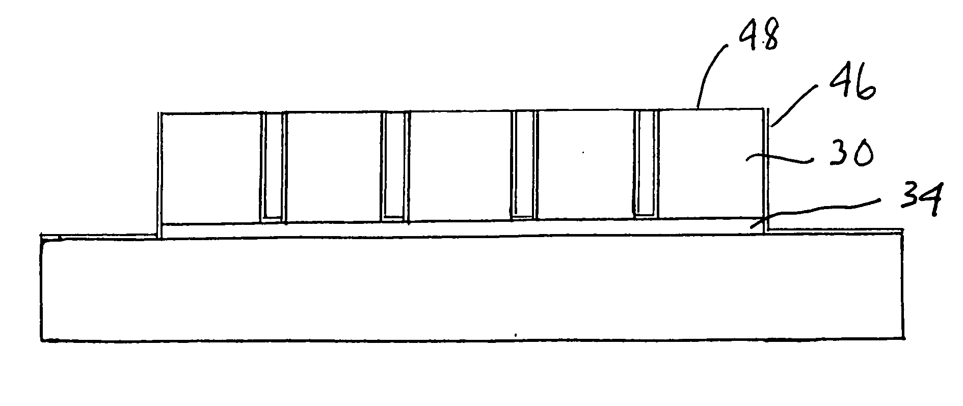
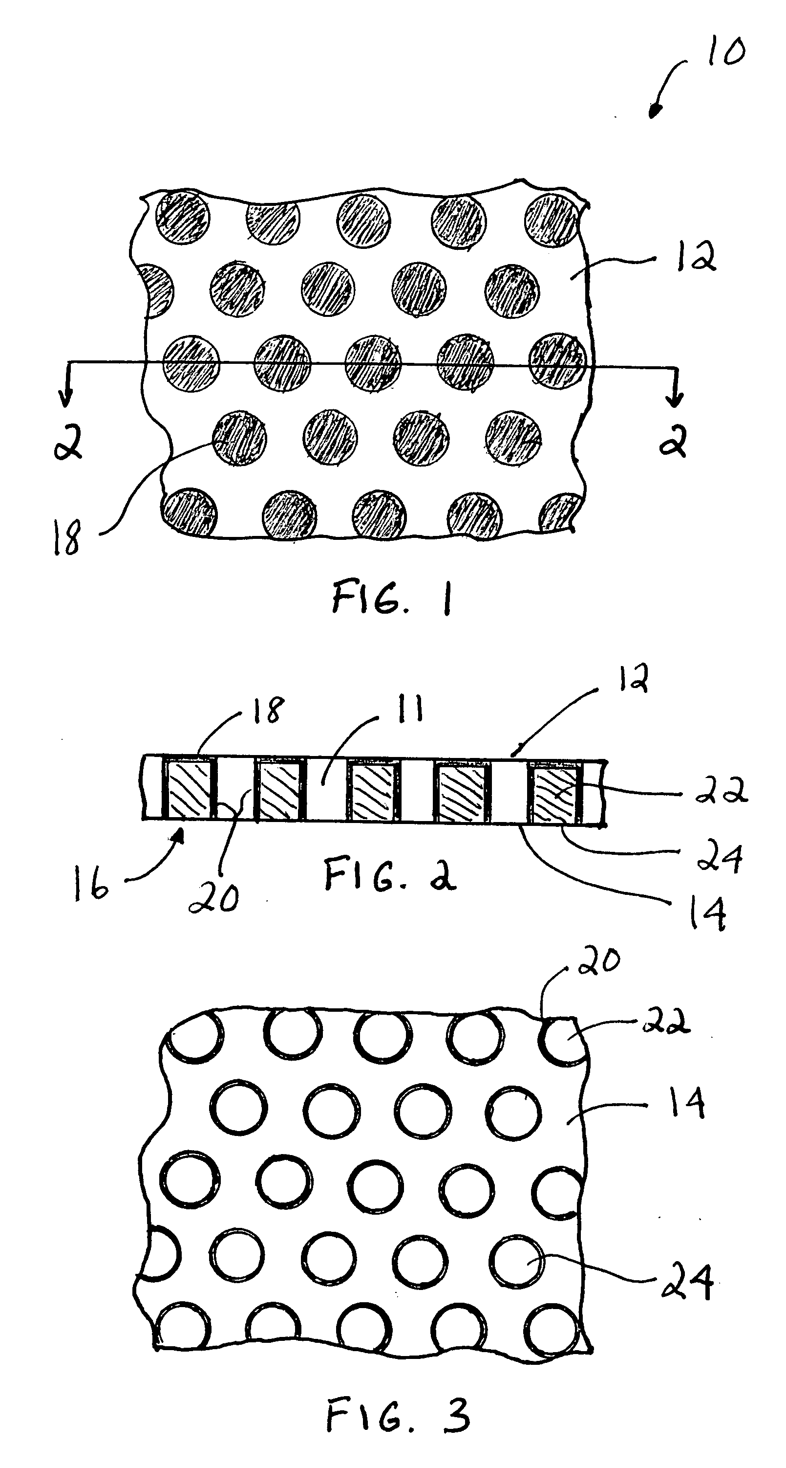
[0025] Referring now to the drawings and particularly to FIGS. 1, 2 and 3, there is shown a semiconductor structure 10 configured in accordance with the invention. The structure 10 includes a substrate 11 having a substantially planar frontside surface 12, a substantially planar backside surface 14 and a plurality of via structures 16. “Planar” as used herein means a surface having a profile that is within a specified deviation tolerance, e.g., within 2-3 microns, that is adequate for further fabrication.

[0026] In a preferred embodiment, the via structures 16 are substantially circular in cross section. In other embodiments the via structures 16 may have anyone of numerous other shapes. The via structure 16 includes a frontside 18 and one or more sidewalls 20. The frontside 18 is substantially planar with respect to the planar frontside surface 12 of the substrate 11 and may be described as forming part of the frontside surface of the structure 10.

[0027] Each of the frontside 18 a...


PUM


Abstract

Methods of backside planarization processes have been developed to gain a high resolution backside process lithography and to make possible the development of dual faced MMICs and circuits. Two different processes have been employed to planarize via structures of various depths, one including epoxy-fill via structures with depths of 10 mils and the other solid-metal via structures with depths of 3.5 mils. Application of a wafer fabricated using methods of the present invention has been demonstrated in a monolithic circuit, where bias control to the frontside of the wafer was established by solder bumps on the planarized backside surface of a wafer including epoxy-filled via structures.

Description

BACKGROUND OF THE INVENTION [0001] 1. Field of the Invention [0002] This invention relates to semiconductor structures including wafers and circuits, and more particularly to semiconductor structures having via structures between planar frontside and backside surfaces. [0003] 2. Description of Related Art [0004] As the application of microwave and millimeter wave products become increasingly more complex, integrated system solutions are required for improving performance criteria. Such solutions typically require a reduction in overall system size which inevitably entails size reductions at the component level. A reduction in system components may be achieved through more efficient utilization of the backside surface of component circuits. [0005] On such application of microwave and millimeter wave products is the electronically steered antenna technology. In this technology active MMIC circuits are incorporated in the antenna itself. See for example, Higgins, J. A.; Hao Xin; Sailer...

Claims


Application Information

Patent Timeline
IPC IPC(8): H01L21/44
CPCH01L21/76898
Inventor KAZEMI, HOOMAN
Owner TELEDYNE LICENSING
Why Eureka
Try Eureka