Small sector floating gate flash memory

a floating gate flash memory and small sector technology, applied in static storage, digital storage, instruments, etc., can solve the problems of large die size penalty, impose overhead expense, and affect the original benefit of the particular p-well, so as to achieve the effect of sacrificing the original benefit and small sector siz

Active Publication Date: 2006-11-16
WINBOND ELECTRONICS CORP
View PDF6 Cites 51 Cited by
  • Summary
  • Abstract
  • Description
  • Claims
  • Application Information

AI Technical Summary

Benefits of technology

[0012] The present invention provides a technique for controlling disturb conditions in floating gate flash memories so that a smaller sector size may be achieved without sacrificing original benefits of this technology. The smaller sector size

Problems solved by technology

The overhead imposed by separate P-wells and the use of respective groups of select transistors for the sectors can result in a big die size penalty if small sectors are implemented.
However, when multiple sectors are created within a particular P-well, and as cells in the particular P-well are programmed or erased by selecting various rows and sectors of cells in the particular P-well over time, the cells in the particular P-well that are not frequently selected suffer from programming disturb and erase disturb.
Disadvantageously, the internal RAM imposes an ove

Method used


Image

  • Small sector floating gate flash memory
  • Small sector floating gate flash memory
  • Small sector floating gate flash memory

Examples


Embodiment Construction

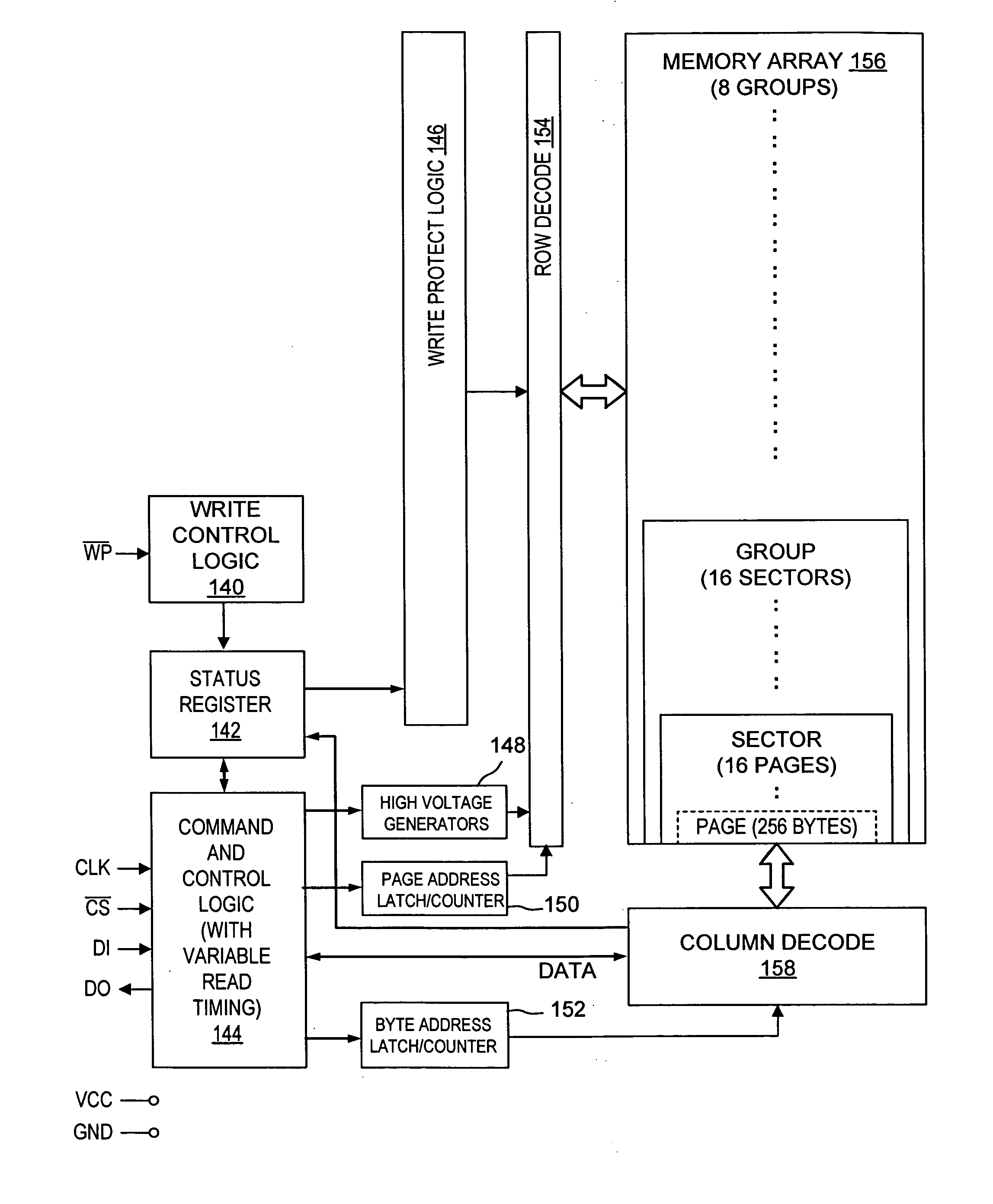
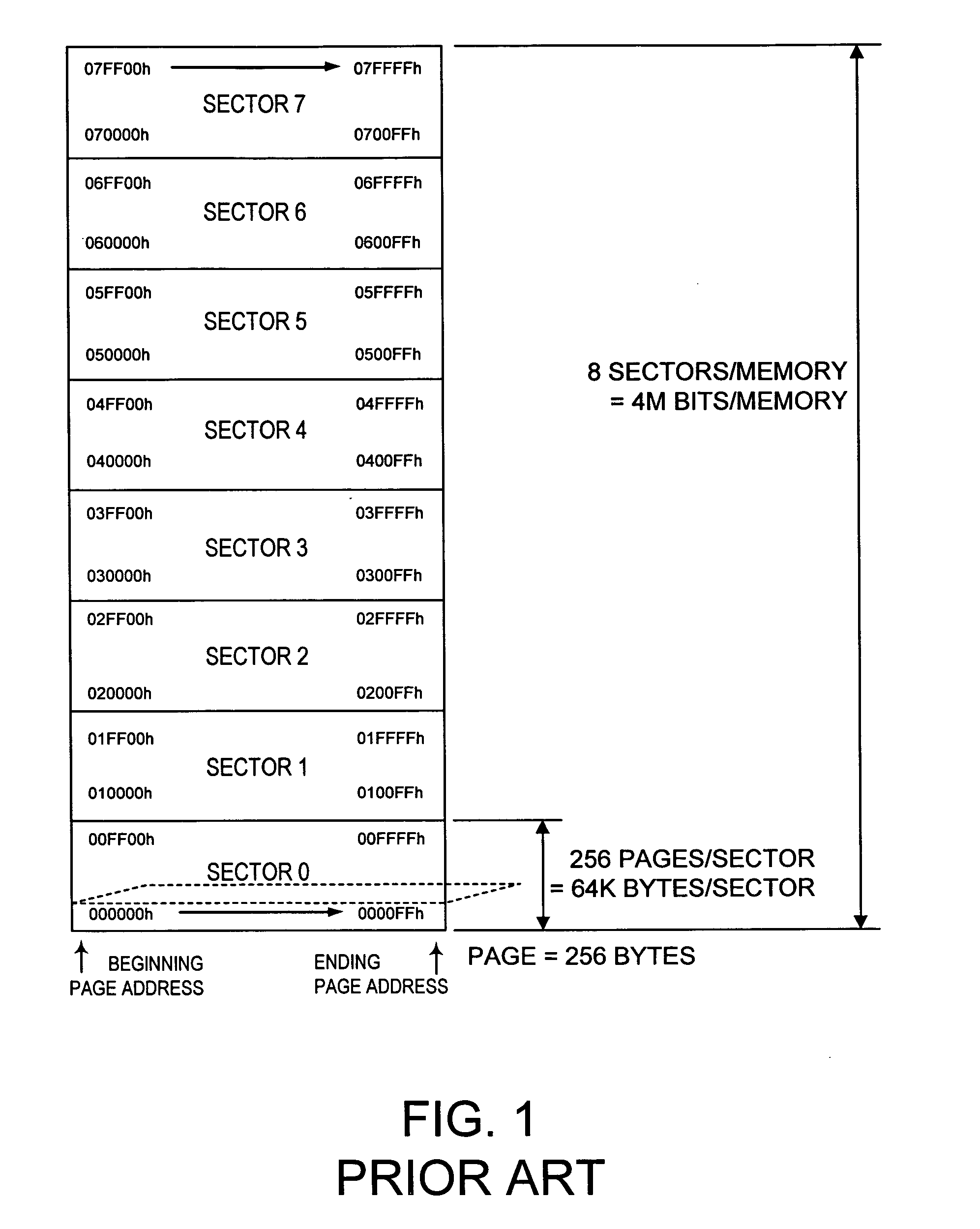
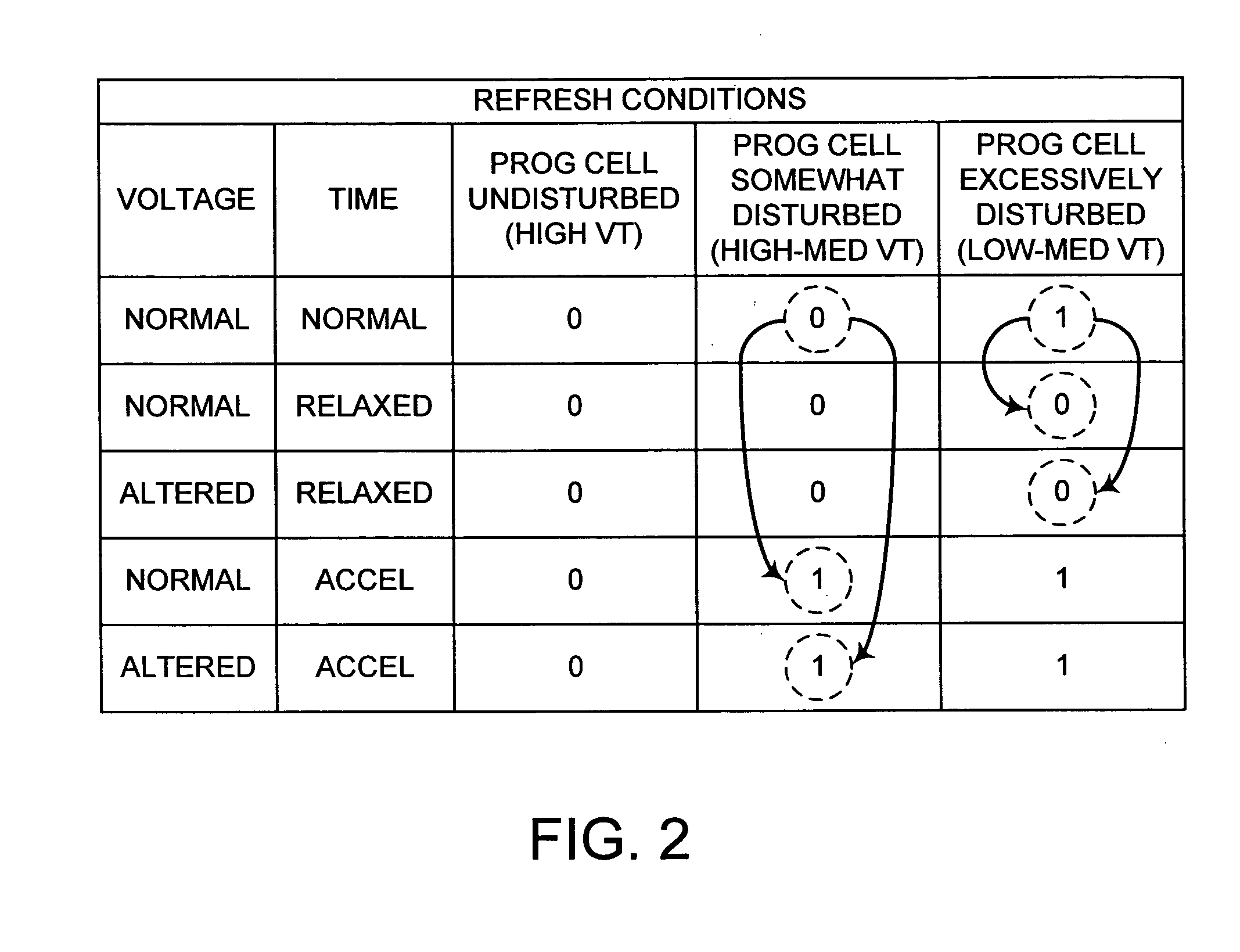
[0042] To control the problem of program and erase disturb in flash memory arrays having multiple sectors of cells grouped in each isolated P-well, a refresh procedure is used that involves two readings of each of the cells in a “refresh area” of a group under different read timing conditions, with other read conditions being constant or varied as desired. Cells that yield the same result in both reads are not excessively disturbed and need not be reprogrammed. However, cells that read differently may be excessively disturbed and should be reprogrammed. The refresh procedure is particularly suitable for memory arrays with small sector size and many sectors per group. The memory arrays preferably incorporate memory cells that use hot electron programming and Fowler-Nordheim erase, and are arranged in a suitable flash architecture such as the well-known NOR common ground architecture or the well-known alternate metal virtual ground architecture. A suitable type of memory cell structur...


PUM


Abstract

To control the problem of program and erase disturb in flash memory arrays having multiple sectors of cells grouped in each isolation wells of the flash memory array, a refresh procedure is used that involves two readings of each of the cells in a “refresh area” of a group under different read timing conditions, with other read conditions being constant or varied as desired. Cells that yield the same result in both reads are not excessively disturbed and need not be reprogrammed. However, cells that read differently may be excessively disturbed and should be reprogrammed. The refresh procedure is particularly suitable for memory arrays with small sector size and many sectors per group. The memory arrays preferably incorporate memory cells that use hot electron programming and Fowler-Nordheim erase.

Description

BACKGROUND OF THE INVENTION [0001] 1. Field of the Invention [0002] The present invention relates to flash semiconductor memory, and more particularly to small sector floating gate flash memory having hot electron programming and Fowler-Nordheim erase. [0003] 2. Description of the Related Art [0004] One common type of floating gate flash memory uses channel hot electron (“CHE”) injection for programming the floating gate memory cells, and Fowler-Nordheim (“FN”) tunneling for erasing the memory cells. Because of small cell size, fast read speed, and good program / erase endurance, floating gate type flash memory is widely used for code storage applications in mobile devices, PC BIOS, and many consumer devices. Floating gate flash memories typically have large sector sizes. FIG. 1 shows an illustrative 4M bit flash memory array that is organized into 2048 programmable pages of 256-bytes each. The pages are grouped into 8 erasable sectors of 256 pages each. The sector size therefore is 6...

Claims


Application Information

Patent Timeline
IPC IPC(8): G11C17/00
CPCG11C16/3418
Inventor PARK, EUNGJOON
Owner WINBOND ELECTRONICS CORP
Why Eureka
Try Eureka