Bi-directional Fowler-Nordheim tunneling flash memory

a flash memory and fowler-nordheim tunneling technology, applied in the field of nonvolatile semiconductor memory, can solve the problems of reducing the duration of batteries used in digital products, decelerating programming speed, and very high power consumption of prior art nand type eeprom b>10/b>, and achieve the effect of prolonging the duration of batteries of portable electric devices

Inactive Publication Date: 2005-01-25
POWERCHIP SEMICON CORP
View PDF10 Cites 22 Cited by
  • Summary
  • Abstract
  • Description
  • Claims
  • Application Information

AI Technical Summary

Benefits of technology

[0008]Accordingly, it is the primary objective of the claimed invention to provide a low-energy consumption nonvolatile memo

Problems solved by technology

However, the above-mentioned flash memory architecture has a drawback in that it consumes a great deal of electricity during a data program operation, leading to a decreased duration of batteries used in digital products.
Consequently, the prior art NAND type EEPROM 10 has very high power consumption.
Furthermore, since high voltages, for example, 20V (for the selected cell) and 12V (for non-selected cells), are required to be applied on the s

Method used


Image

  • Bi-directional Fowler-Nordheim tunneling flash memory
  • Bi-directional Fowler-Nordheim tunneling flash memory
  • Bi-directional Fowler-Nordheim tunneling flash memory

Examples


Embodiment Construction

ent of the present invention.

[0029]FIG. 11(a) and FIG. 11(b) are a cross-sectional schematic diagram illustrating a BiNOR EEPROM cell and exemplary operation modes thereof (erase, program, and read operations, respectively) according to the fifth preferred embodiment of this invention.

[0030]FIG. 12(a) to FIG. 12(c) are segmental circuit arrangement of the BiNOR EEPROM and exemplary operation modes thereof (erase, program, and read operations, respectively) according to the fifth preferred embodiment of this invention.

[0031]FIG. 13 and FIG. 14 illustrate other embodiments according to this invention.

DETAILED DESCRIPTION

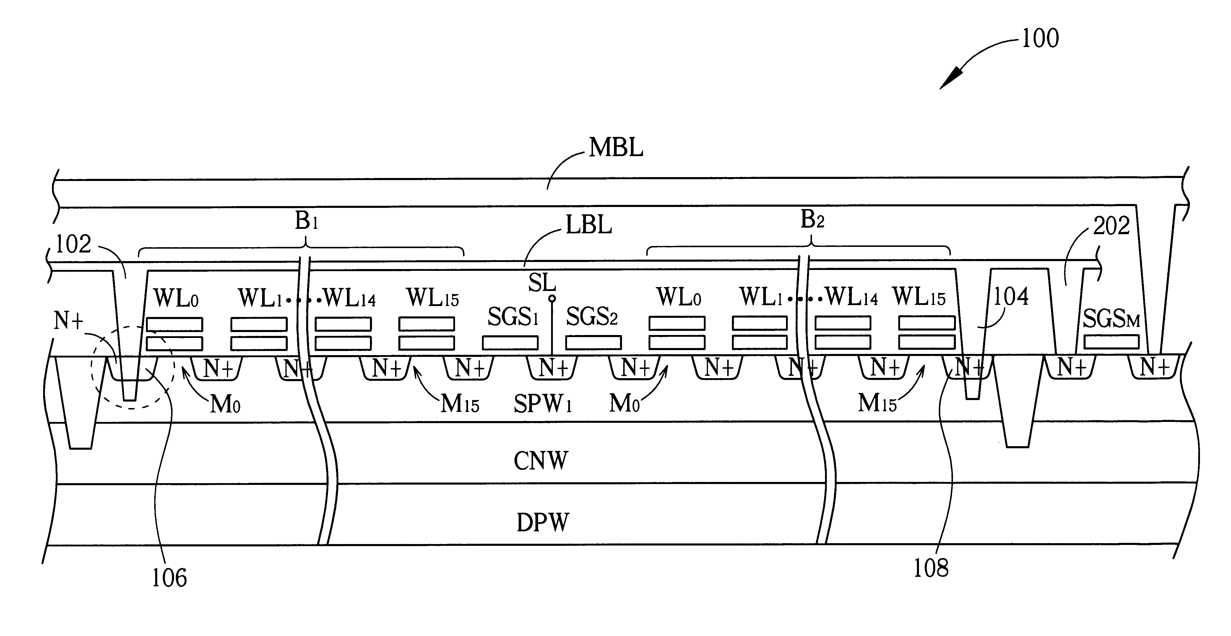
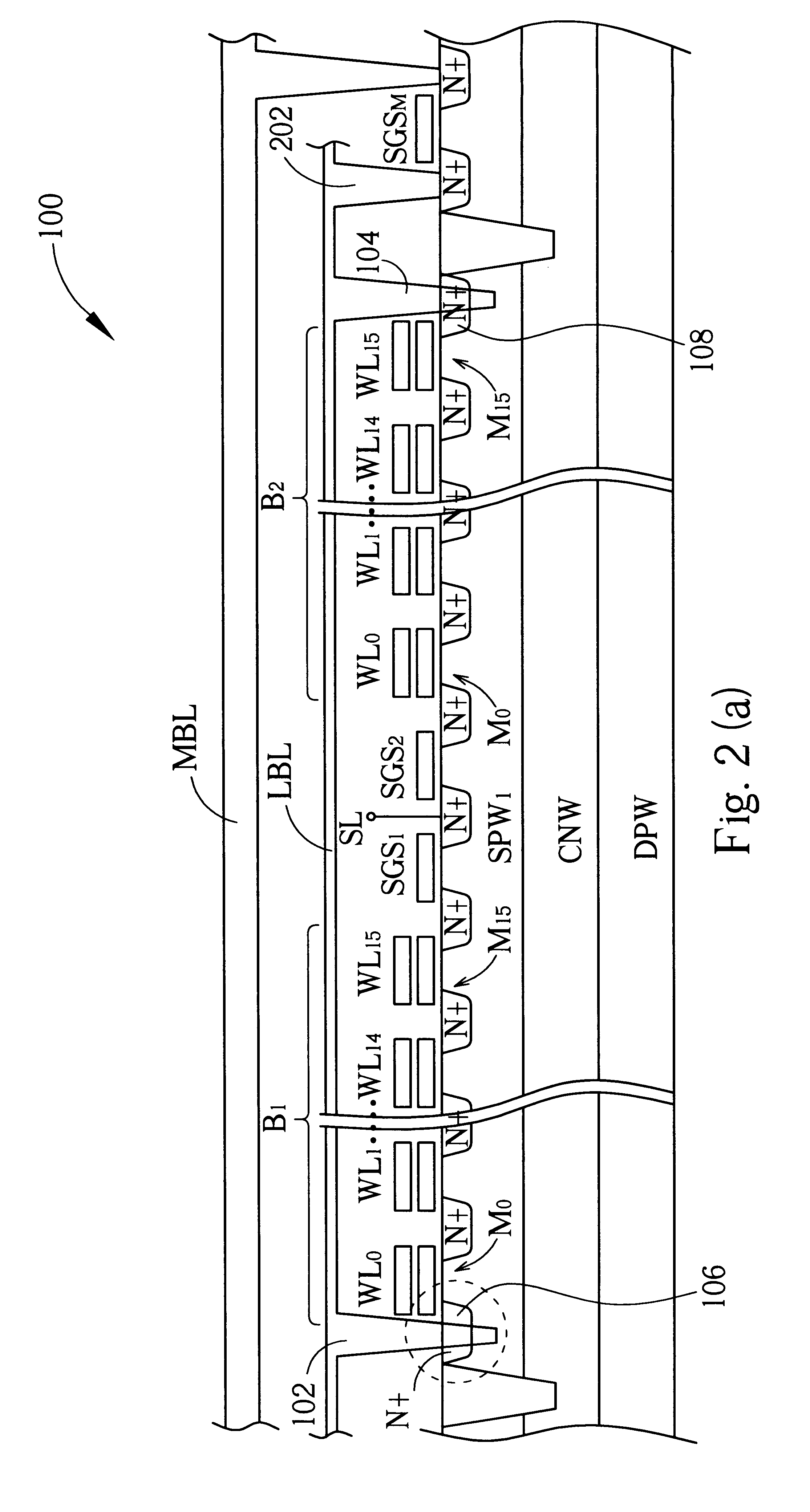
[0032]Referring to FIG. 2(a), a portion of an EEPROM 100 is shown in a cross-sectional view according to the first preferred embodiment of this invention in which only two series connected NAND memory cell blocks B1 and B2 are illustrated for the sake of simplicity. As shown in FIG. 2(a), the EEPROM 100, which is based on a novel low-voltage bi-directional FN write / era...


PUM


Abstract

A low-voltage nonvolatile memory array includes a cell well of a first conductivity type formed in a substrate; columns of buried bit lines of a second conductivity type formed within the cell well, wherein columns of the buried bit lines are isolated from each other and each is further divided into of sub-bit line segments with deeply doped source wells of the first conductivity type connected to the cell well; a plurality of memory cell blocks serially arranged over one of the columns of buried bit lines, wherein a memory cell block corresponds to a sub-bit line segment, and each memory cell block includes at least one memory transistor having a stacked gate, source, and drain; and a local bit line overlying the memory cell blocks and electrically connected to the drain of the memory transistor via a contact plug short-circuiting the drain and the subjacent buried bit line.

Description

BACKGROUND OF INVENTION[0002]1. Field of the Invention[0003]The present invention relates to a nonvolatile semiconductor memory, and more particularly, to a bi-directional Fowler-Nordheim (FN) write / erase flash memory utilizing a compatible and low-electric consumption operation mode. According to the present invention, high-speed code flash memory and high-density data flash memory can be integrated on a single chip.[0004]2. Description of the Prior Art[0005]Recently, flash electrically erasable programmable read-only memories (EEPROMs) have gained substantial interest as the best solution for electrically rewritable nonvolatile data storage. These semiconductor memories, which have been broadly used on digital products such as digital cameras, cell phones, video game apparatuses, personal digital assistants (PDA), and so on, combine the high integration density and the high programming speed of EPROMs with the higher functionality of EEPROMs by offering electrical in-circuit erasa...

Claims


Application Information

Patent Timeline
IPC IPC(8): H01L29/66H01L27/115H01L21/70H01L21/8247H01L29/788G11C16/04
CPCH01L29/7883H01L27/11521H01L27/11524H01L27/115G11C16/0433G11C16/0483H10B41/35H10B69/00H10B41/30
Inventor YANG, CHING-SUNGSHEN, SHIH-JYEHSU, CHING-HSIANG
Owner POWERCHIP SEMICON CORP
Why Eureka
Try Eureka