High-voltage transistor fabrication with trench etching technique

a technology of trench etching and high-voltage transistors, which is applied in the direction of transistors, semiconductor devices, semiconductor/solid-state device details, etc., can solve the problems of limiting the current-carrying capability available for a given footprint or cost, and the amount of active channels is limited by the surface area of the die, so as to achieve the effect of particularly easy depletion-mode device fabrication

Active Publication Date: 2006-11-23
BOURNS INC
View PDF4 Cites 46 Cited by
  • Summary
  • Abstract
  • Description
  • Claims
  • Application Information

AI Technical Summary

Benefits of technology

[0006] The disclosed innovations, in various embodiments, provide one or more of at least the following advantages:
[0008] The total current-switching capability for a given footprint can be increased.
[0009] The total current-switching capability for a single die can be increased.
[0010] The heat dissipation for a given process flow and footprint can be decreased.
[0011] By addition of a deep trench etch, an integrated power process can obtain high current-switching capability.

Problems solved by technology

However, MOSFET and JFET structures that are manufactured with their channel regions at the top surface of the die have the amount of active channel limited by the surface area of the die.
This limits the current-carrying capability available for a given footprint or cost.

Method used


Image

  • High-voltage transistor fabrication with trench etching technique
  • High-voltage transistor fabrication with trench etching technique
  • High-voltage transistor fabrication with trench etching technique

Examples


Embodiment Construction

[0021] The numerous innovative teachings of the present application will be described with particular reference to the presently preferred embodiment (by way of example, and not of limitation).

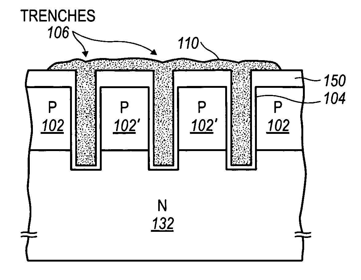
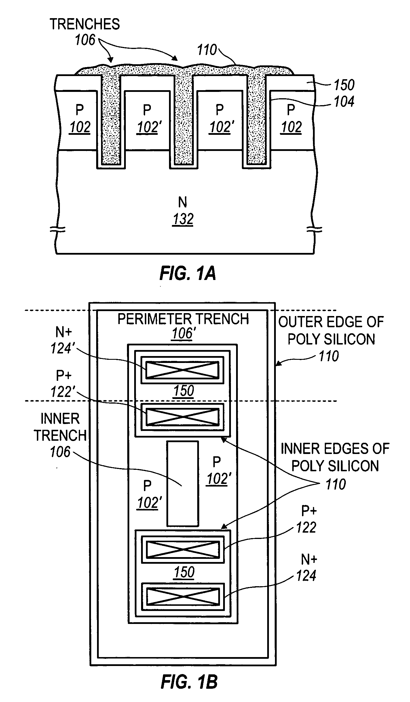
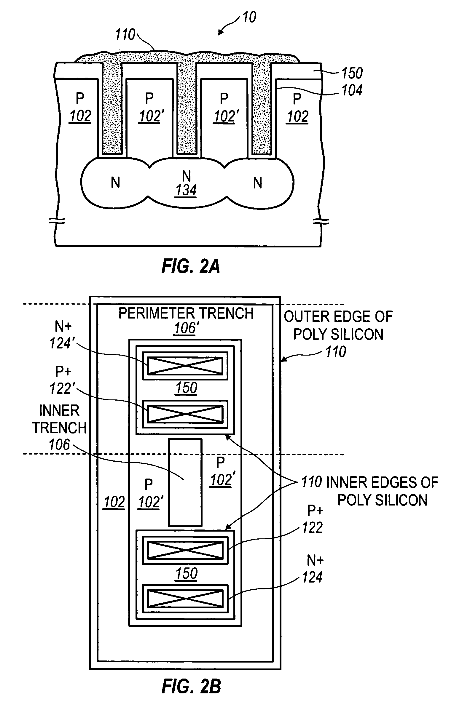
[0022] The present application describes techniques for significantly increasing the amount of active channel that can be obtained on a die through the use of trench technology for JFETs and depletion mode MOSFETs. An earlier U.S. Pat. No. 4,393,391, describes the manufacture of enhancement mode power MOS transistors, including DMOS transistors that have the amount of active channel area increased through the use of grooves having various geometries. The present invention disclosure differs considerably from the devices described in this earlier patent, as will be described below.

[0023] Depletion mode MOSFETs have a channel region present when no gate-to-source voltage is applied. Applying a voltage of the appropriate polarity to the gate decreases the conductivity of the channel. The amount...


PUM


Abstract

A lateral high-voltage depletion-mode device structure in which fingers of semiconductor material are interdigitated with trench gates. Since the effective channel area is proportional to the depth of the trenches, a large amount of active channel area can be achieved for a given surface area.

Description

CROSS-REFERENCE TO RELATED APPLICATIONS [0001] This application claims priority from U.S. provisional patent application 60 / 626,374 filed on Nov. 9, 2004, which is hereby incorporated by reference.BACKGROUND AND SUMMARY OF THE INVENTIONS [0002] The present application relates to semiconductor devices, and more particularly to devices which are capable of switching relatively high voltages, e.g. of 50V or more, while remaining reasonably compatible with integrated circuit fabrication techniques. [0003] Many power devices are designed as vertical devices, where the direction of carrier flow is into the semiconductor material (normal to the surface of the wafer). However, there are many advantages to “lateral” power devices, i.e. to transistors which have their direction of carrier flow approximately parallel to the surface. One outstanding attraction of lateral devices is process compatibility, since lateral devices can usually be fabricated with process steps which are the similar to...

Claims


Application Information

Patent Timeline
Patent Type & Authority Applications(United States)
IPC IPC(8): H01L29/94H01L21/336
CPCH01L23/535H01L29/0626H01L29/0646H01L29/0692H01L29/1066H01L29/2003H01L29/4236H01L2924/0002H01L29/4238H01L29/7838H01L29/808H01L2924/00
Inventor BLANCHARD, RICHARD A.HEBERT, FRANCOISE
Owner BOURNS INC
Why Eureka
Try Eureka