Radio frequency switching circuit and semiconductor device including the same

Inactive Publication Date: 2006-11-23
PANASONIC CORP
View PDF1 Cites 37 Cited by
  • Summary
  • Abstract
  • Description
  • Claims
  • Application Information

AI Technical Summary

Benefits of technology

[0011] Therefore, an object of the present invention is to provide a radio frequency switching circuit having

Problems solved by technology

In actuality, however, the inter-stage potentials between the plurality of FETs in an OFF state cannot be at an equal level merely by connecting a resistor having a high resistance value to each FET in parallel.
This causes a problem that when a high power signal

Method used


Image

  • Radio frequency switching circuit and semiconductor device including the same
  • Radio frequency switching circuit and semiconductor device including the same
  • Radio frequency switching circuit and semiconductor device including the same

Examples


first embodiment

[0050] With reference to FIG. 1 through FIG. 5, a radio frequency switching circuit according to a first embodiment of the present invention will be described. A semiconductor device according to this embodiment includes the radio frequency switching circuit shown in FIG. 1 integrated on a semiconductor substrate.

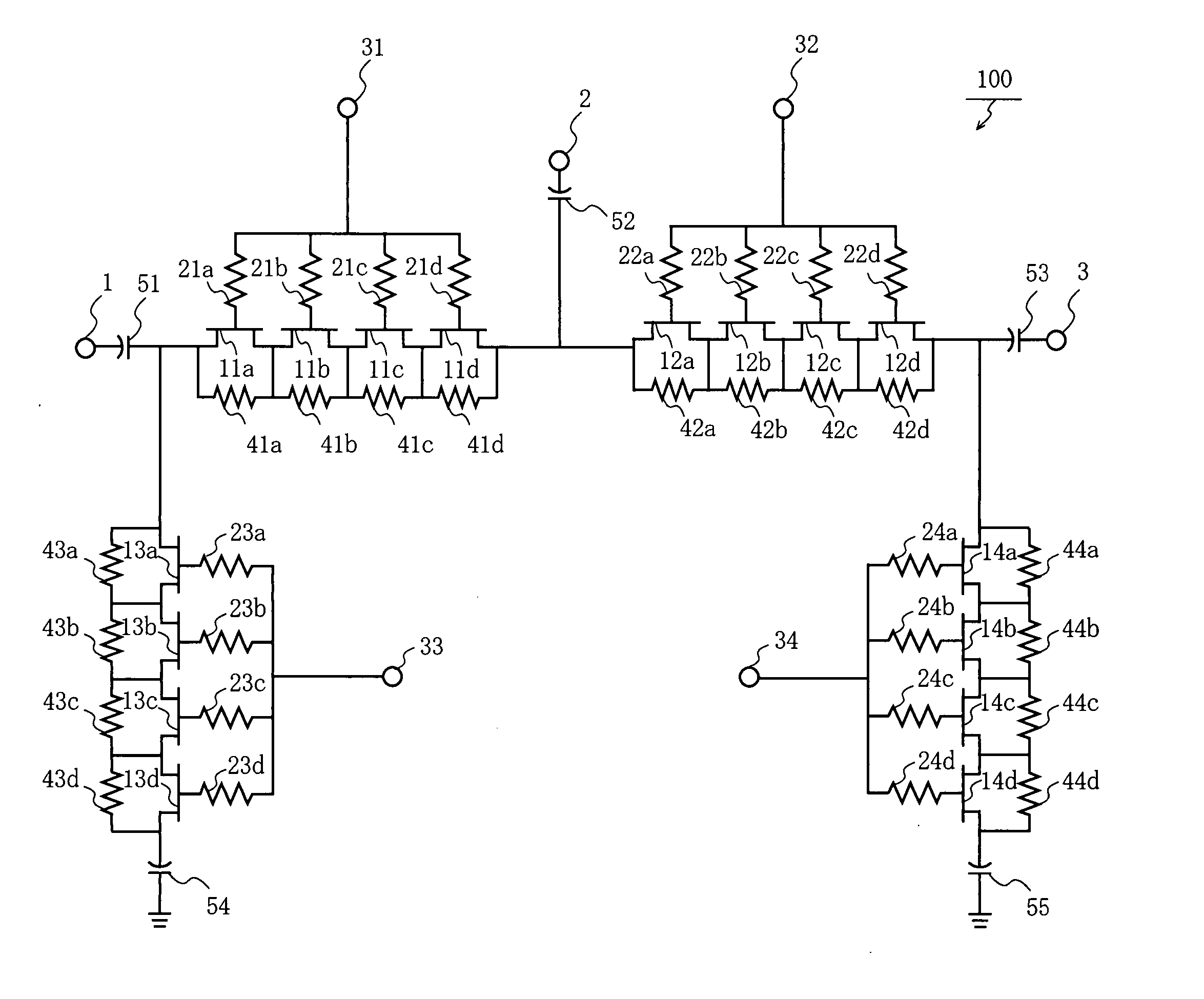
[0051]FIG. 1 is a circuit diagram of a radio frequency switching circuit according to the first embodiment of the present invention. A radio frequency switching circuit 100 shown in FIG. 1 includes FETs 11a through 11d, 12a through 12d, 13a through 13d and 14a through 14d, gate bias resistors 21a through 21d, 22a through 22d, 23a through 23d and 24a through 24d, inter-stage potential fixing resistors 41a through 41d, 42a through 42d, 43a through 43d and 44a through 44d, capacitors 51 through 55, first through third input / output terminals 1 through 3, and first through fourth control terminals 31 through 34. The first through third input / output terminals 1 through 3 are pro...

second embodiment

[0069] With reference to FIG. 6 through FIG. 9, a radio frequency switching circuit according to a second embodiment of the present invention will be described. A semiconductor device according to this embodiment includes the radio frequency switching circuit shown in FIG. 6 integrated on a semiconductor substrate.

[0070]FIG. 6 is a circuit diagram of a radio frequency switching circuit according to the second embodiment of the present invention. A radio frequency switching circuit 200 shown in FIG. 6 includes FETs 11a through 11d, 12a through 12d, 13a through 13d and 14a through 14d, gate bias resistors 21a through 21d, 22a through 22d, 23a through 23d and 24a through 24d, inter-stage potential fixing resistors 41e through 41h, 42e through 42h, 43e through 43h and 44e through 44h, capacitors 51 through 55, 61a through 61d, 62a through 62d, 63a through 63d and 64a through 64d, first through third input / output terminals 1 through 3, and first through fourth control terminals 31 throu...

third embodiment

[0087] With reference to FIG. 10 through FIG. 13, a radio frequency switching circuit according to a third embodiment of the present invention will be described. In the radio frequency switching circuit according to this embodiment, the FETs connected in a plurality of stages in the first embodiment are replaced with multi-gate FETs (dual-gate FETs in this example). A semiconductor device according to this embodiment includes the radio frequency switching circuit shown in FIG. 10 integrated on a semiconductor substrate.

[0088]FIG. 10 is a circuit diagram of a radio frequency switching circuit according to the third embodiment of the present invention. A radio frequency switching circuit 300 shown in FIG. 10 includes multi-gate FETs 101a, 101b, 102a, 102b, 103a, 103b, 104a and 104b, gate bias resistors 121a through 121d, 122a through 122d, 123a through 123d and 124a through 124d, inter-stage potential fixing resistors 111a through 111c, 112a through 112c, 113a through 113c and 114a t...


PUM


Abstract

A radio frequency switching circuit having improved input/output power characteristics is provided. The circuit includes basic switching sections each including a plurality of FETs 13a-13d, 14a-14d, 11a-11d or 12a-12d connected in series. The basic switching sections are respectively provided between an input/output terminal 1 and the ground, between an input/output terminal 3 and the ground, between the input terminals 1 and 2, and between the input terminals 2 and 3. The circuit also includes a plurality of resistors 43a-43d, 44a-44d, 41a-41d and 42a-42d, each having one terminal connected to a drain electrode of a corresponding FET and the other terminal connected to a source electrode of the corresponding FET. A resistor connected between the drain and source electrodes of an FET, among the FETs included in a basic switching section in an OFF state, closer to the input/output terminal to which a signal is inputted has a smaller resistance value.

Description

BACKGROUND OF THE INVENTION [0001] 1. Field of the Invention [0002] The present invention relates to a radio frequency switching circuit, and more specifically to a radio frequency switching circuit using a field effect transistor. [0003] 2. Description of the Background Art [0004] In recent years, as wireless terminals and the like have rapidly prevailed and enhanced, radio frequency switching circuits used in the wireless terminals and the like now require having low-loss and low-distortion characteristics. Under such circumstances, radio frequency switching circuits including field effect transistors (hereinafter, referred to as “FETS”) connected in a plurality of stages have been conventionally proposed. One example of such radio frequency switching circuits is described in Japanese Laid-Open Patent Publication No. 2000-277703. [0005]FIG. 16 shows a radio frequency switching circuit described in Japanese Laid-Open Patent Publication No. 2000-277703. The radio frequency switching...

Claims


Application Information

Patent Timeline
IPC IPC(8): H01P1/15H03K17/00
CPCH03K17/693H03K17/6871
Inventor MIYAGI, MASASHINAKATSUKA, TADAYOSHI
Owner PANASONIC CORP
Why Eureka
Try Eureka