Display device

a display device and display pixel technology, applied in the field of display devices, can solve the problems of affecting the further lowering of power consumption, affecting the display device's display quality, and unable to achieve the effect of reducing the incidence of defective panels, and reducing the degradation of display quality of display pixels

Active Publication Date: 2006-11-30
SANYO ELECTRIC CO LTD
View PDF1 Cites 50 Cited by
  • Summary
  • Abstract
  • Description
  • Claims
  • Application Information

AI Technical Summary

Benefits of technology

[0038] As described above, with a display device according to the present invention, a defective pixel can be made inconspicuous. This helps alleviate degradation in the display quality of the display pixel, and helps reduce the incidence of defective panels.

Problems solved by technology

For application in cellular phones, digital still cameras, and the like, however, such display devices are still to attain lower power consumption.
This results in poor light use efficiency, hampering further lowering of power consumption.
This not only degrades the display quality of the display panel, but also increases the incidence of defective panels, leading to a low yield.
Thus, with no black spot appearing, the defect is comparatively inconspicuous.

Method used


Image

  • Display device
  • Display device
  • Display device

Examples


first embodiment

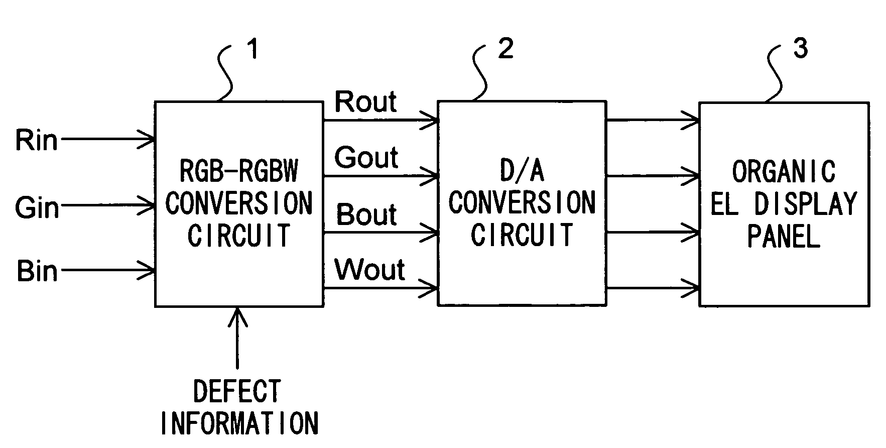
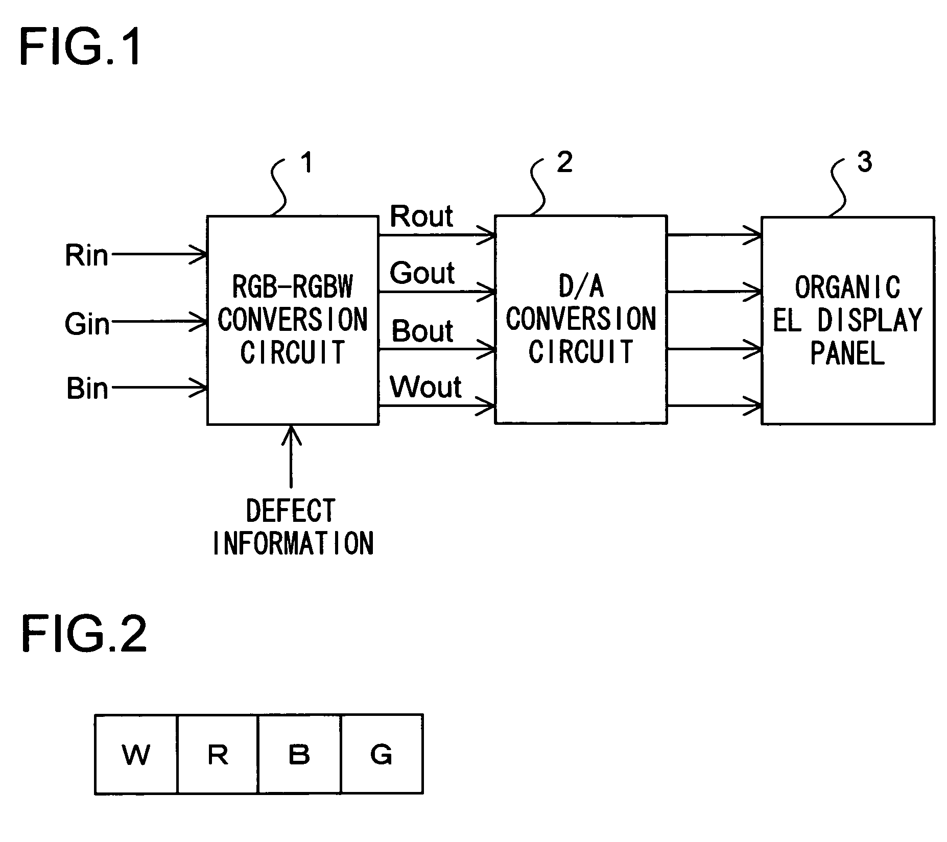
[0066] A first embodiment of the present invention will be described in detail below with reference to the accompanying drawings. FIG. 1 shows the configuration of an organic EL (electroluminescence) display device of the first embodiment of the present invention. As shown in FIG. 1, the organic EL display device of the first embodiment includes an RGB-RGBW conversion circuit 1, a D / A conversion circuit 2, and an organic EL display panel 3 (hereinafter referred to simply as the “display panel 3”). The organic EL display device of this embodiment further includes a defect position specifier 15 and other components (see FIG. 6), which are omitted from illustration in FIG. 1.

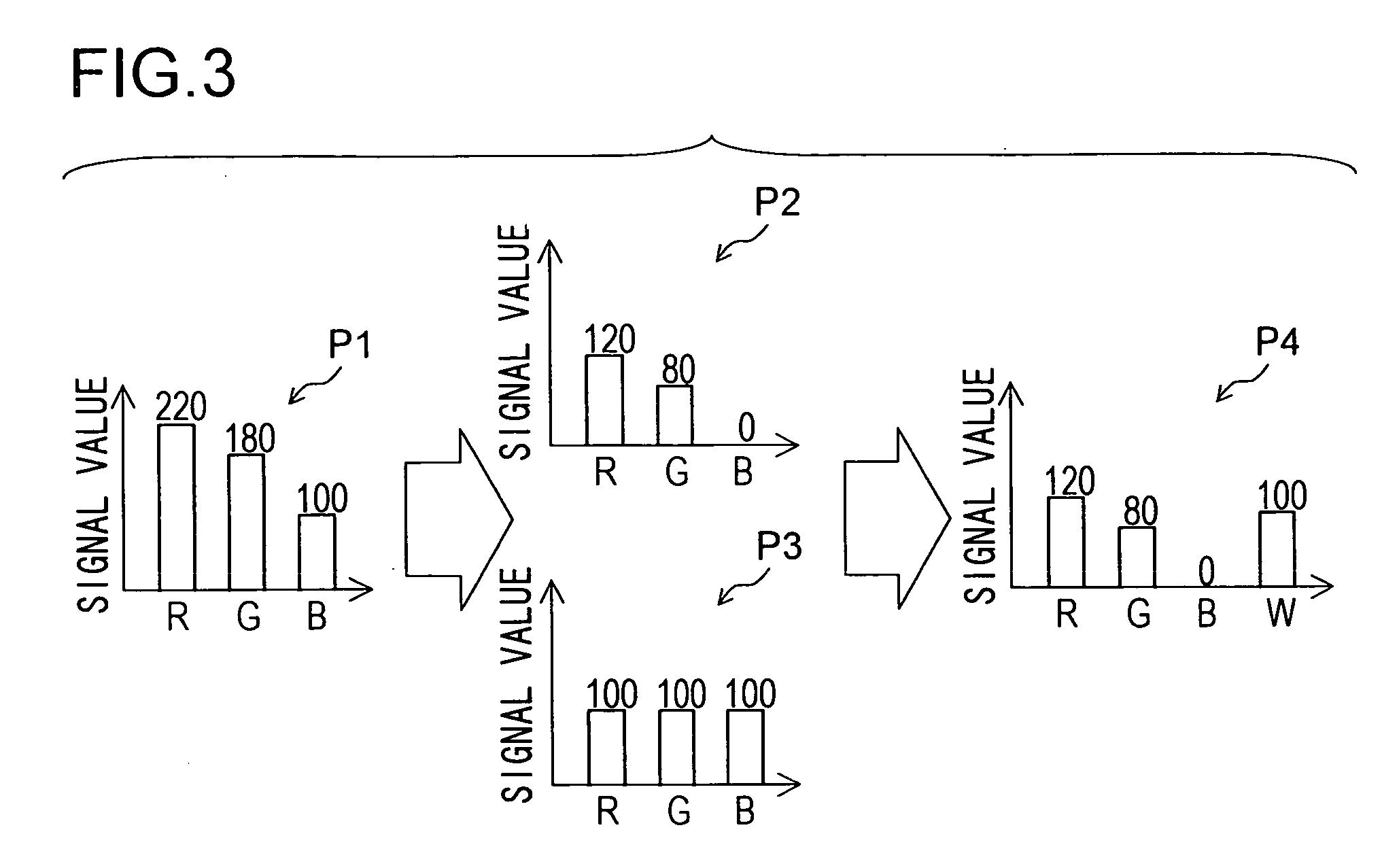
[0067] From outside, digital RGB signals Rin, Gin, and Bin are fed to the RGB-RGBW conversion circuit 1. In the following description, these RGB signals Rin, Gin, and Bin are also referred to simply as the “RGB input signals”. Based on pixel defect information fed from the defect position specifier 15 (see FIG. 6)...

second embodiment

[0150] Next, a second embodiment of the present invention will be described in detail with reference to the accompanying drawings. FIG. 17 shows the configuration of an organic EL display device of the second embodiment of the present invention. In FIG. 17, such parts as are found also in FIG. 1 are identified with common reference numerals and symbols, and no overlapping description will be repeated. As shown in FIG. 17, the organic EL display device of the second embodiment includes an RGB-RGBW conversion circuit 1, a D / A conversion circuit 2, and an organic EL display panel 3a (hereinafter referred to simply as the “display panel 3a”). The organic EL display device of the second embodiment is thus different from the organic EL display device of the first embodiment in that the display panel 3 is replaced with the display panel 3a, and is otherwise configured similarly thereto. The organic EL display device of this embodiment further includes a defect position specifier 15 and oth...


PUM

PropertyMeasurementUnit
brightness LWtaaaaaaaaaa
coloraaaaaaaaaa
brightnessaaaaaaaaaa

Abstract

A display device has: an RGB-RGBW conversion circuit that converts RGB signals fed thereto into RGBW signals; a display panel that has a plurality of dots each composed of four, namely R, G, B, and W, unit pixels and that displays an image based on the RGBW signals; a defect position specifier that specifies, if a unit pixel is found defective, a position of the defective pixel on the display panel; and a conversion rate controller that controls the rate at which, when the RGB signals are converted into the RGBW signals, the RGB signals are converted into a W signal according to the position of the defective pixel. If the defective pixel is a W pixel, the conversion rate for pixels adjacent thereto is made lower than the standard conversion rate set for the entire display panel.

Description

[0001] This application is based on Japanese Patent Application No. 2005-152058 filed on May 25, 2005, the contents of which are hereby incorporated by reference. BACKGROUND OF THE INVENTION [0002] 1. Field of the Invention [0003] The present invention relates to a display device such as an organic EL (electroluminescence) display device, inorganic EL display device, liquid crystal display device, or plasma display device. [0004] 2. Description of Related Art [0005] Display devices like an organic EL display device provided with a self-luminous display panel (self-luminous display) offer advantages of being slim, lightweight, and low-power-consumption, and have been finding increasingly wide application. For application in cellular phones, digital still cameras, and the like, however, such display devices are still to attain lower power consumption. [0006] There have been developed RGB-type organic EL display devices having R, G, and B color filters bonded to a white light emitting ...

Claims


Application Information

Patent Timeline
Patent Type & Authority Applications(United States)
IPC IPC(8): G09G5/02G02F1/133G09G3/20G09G3/30H01L51/50H05B33/12
CPCG09G3/2003G09G3/3208G09G2360/16G09G2320/0242G09G2330/08G09G2300/0452G09G2340/06
Inventor TANASE, SUSUMUYAMASHITA, ATSUHIROMORI, YUKIOMURATA, HARUHIKOMARUMO, KOJIMAMENO, KAZUNOBU
Owner SANYO ELECTRIC CO LTD
Why Eureka
Try Eureka