Plastic integrated circuit package, leadframe and method for use in making the package
- Summary
- Abstract
- Description
- Claims
- Application Information
AI Technical Summary
Problems solved by technology
Method used
Image

Examples
Example
[0021] The present invention is directed towards an improved plastic package for housing a semiconductor device, and a method of making such a package. The packages of the present invention are more efficiently-sized and characteristically optimized than conventional packages
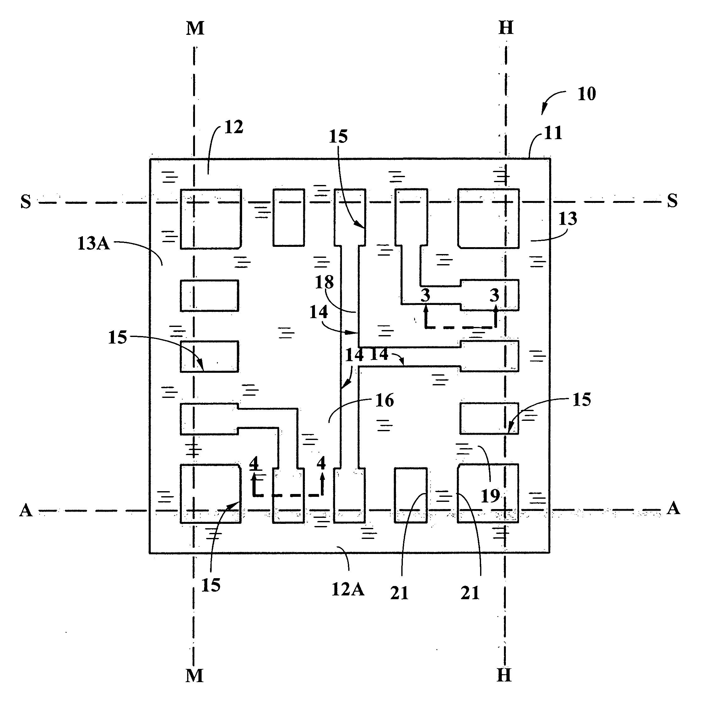
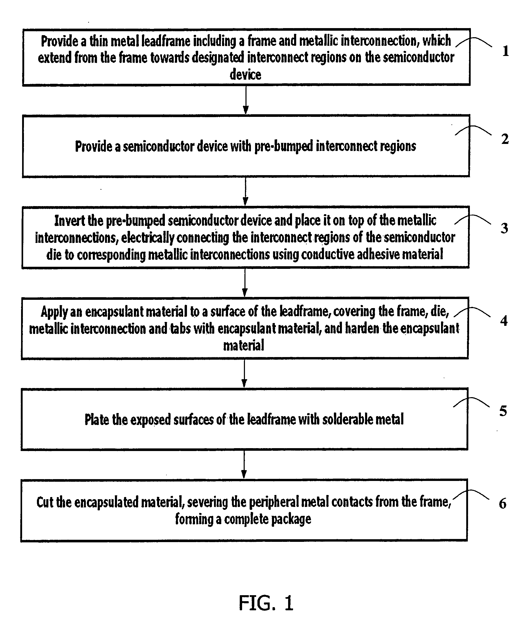
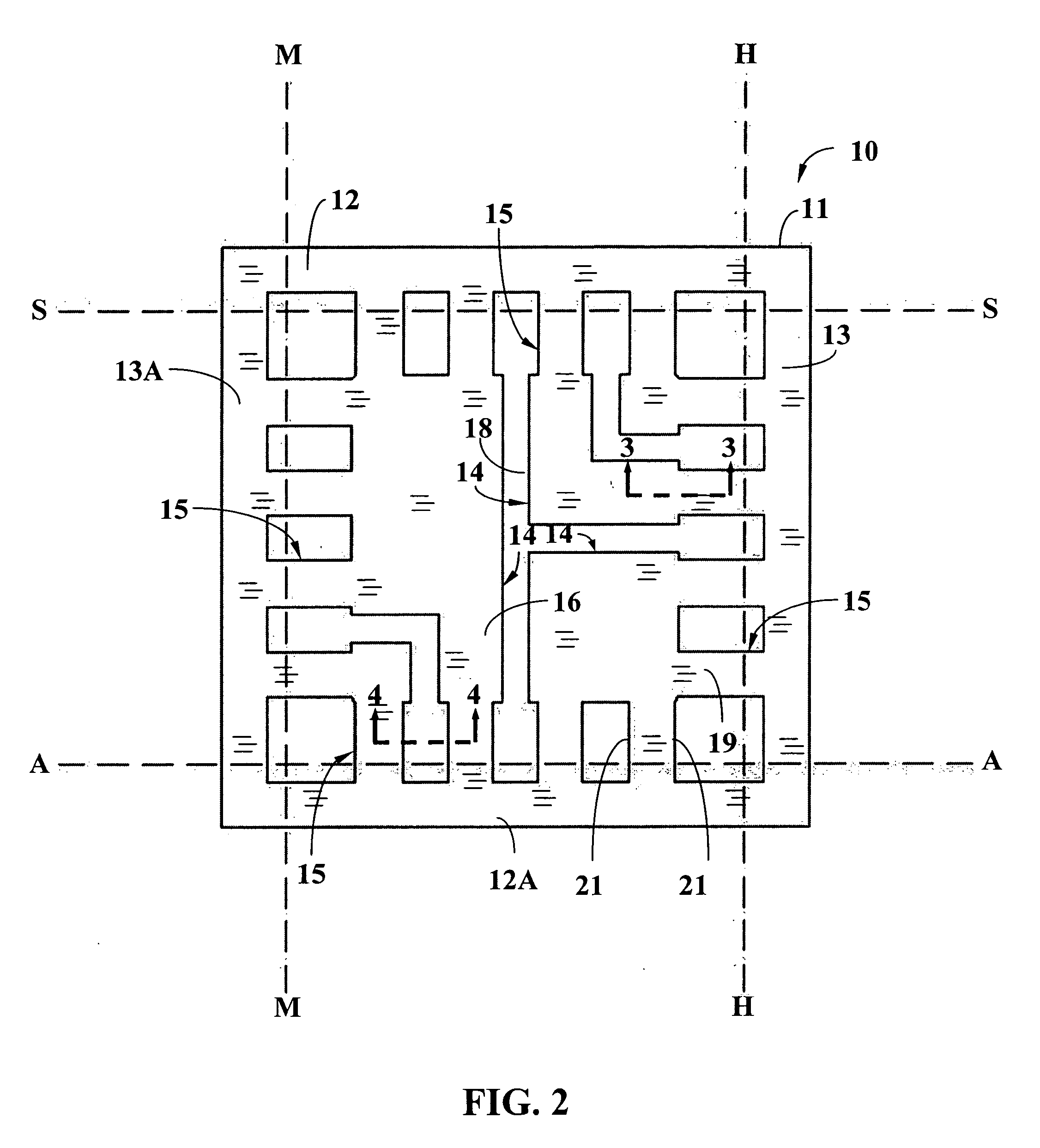
[0022] In one embodiment of the assembly method for a package within the present invention, Step 1 provides a metal leadframe. The leadframe includes a rectangular frame, with a plurality of metal tabs and extended metallic interconnections. The number and location of the metal tabs and extended metallic interconnections may vary, depending on the semiconductor device design configuration. The tabs and extended metallic interconnections have peripheral side surfaces, which may include a reentrant portion(s) and asperities which enhance the connection between tabs and extended metallic interconnections to the encapsulant. The extended metallic interconnections are connected to designate tabs and are extending to...
PUM
 Abstract
Description
Claims
Application Information
 - R&D Engineer
- R&D Manager
- IP Professional
- Industry Leading Data Capabilities
- Powerful AI technology
- Patent DNA Extraction
Browse by: Latest US Patents, China's latest patents, Technical Efficacy Thesaurus, Application Domain, Technology Topic.
© 2024 PatSnap. All rights reserved.Legal|Privacy policy|Modern Slavery Act Transparency Statement|Sitemap