Method for manufacturing semiconductor device

a manufacturing method and semiconductor technology, applied in the direction of hot plate heating arrangement, polycrystalline material growth, crystal growth process, etc., can solve the problems of low thermal absorption efficiency, low thermal conductivity of substrate, and difference in temperature between front and back surfaces

Inactive Publication Date: 2006-10-26
LAPIS SEMICON CO LTD
View PDF2 Cites 392 Cited by
  • Summary
  • Abstract
  • Description
  • Claims
  • Application Information

AI Technical Summary

Problems solved by technology

Thus, when the manufacturing process using the silicon wafer is diverted to the manufacturing process using the sapphire wafer, a problem arises which results from the fact that the sapphire substrate is low in thermal conductivity as compared with the silicon substrate and thermal absorption efficiency is low due to non-absorption of light in a range from visible light to infrared light.
However, the above related art is accompanied by problems that in an atmospheric-pressure CVD apparatus employed in a manufacturing process in which since the sapphire substrate is heated from the back surface of the sapphire wafer, an atmosphere temperature in the corresponding process is low and the heating of the sapphire substrate is necessary, e.g., a process based on an atmospheric-pressure CVD (Chemical Vapor Deposition) method, a difference in tempera

Method used


Image

  • Method for manufacturing semiconductor device
  • Method for manufacturing semiconductor device
  • Method for manufacturing semiconductor device

Examples


first preferred embodiment

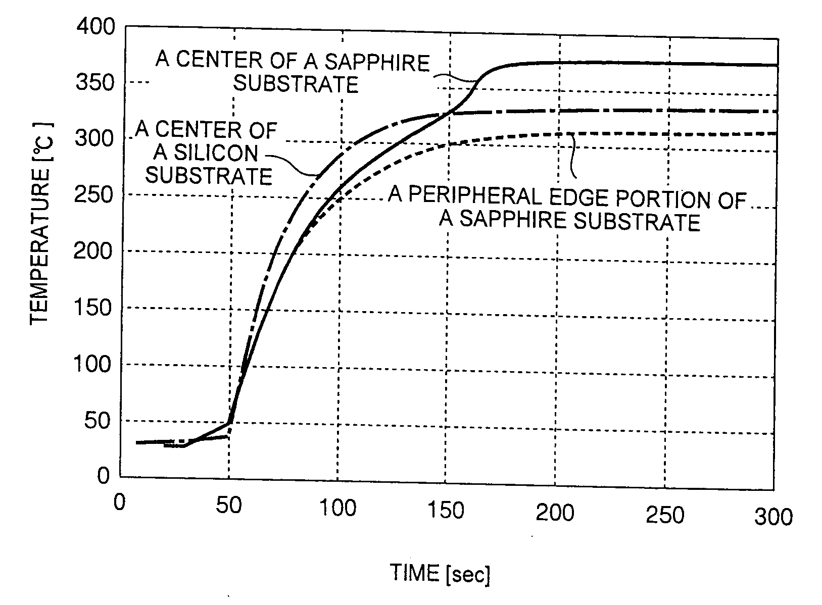
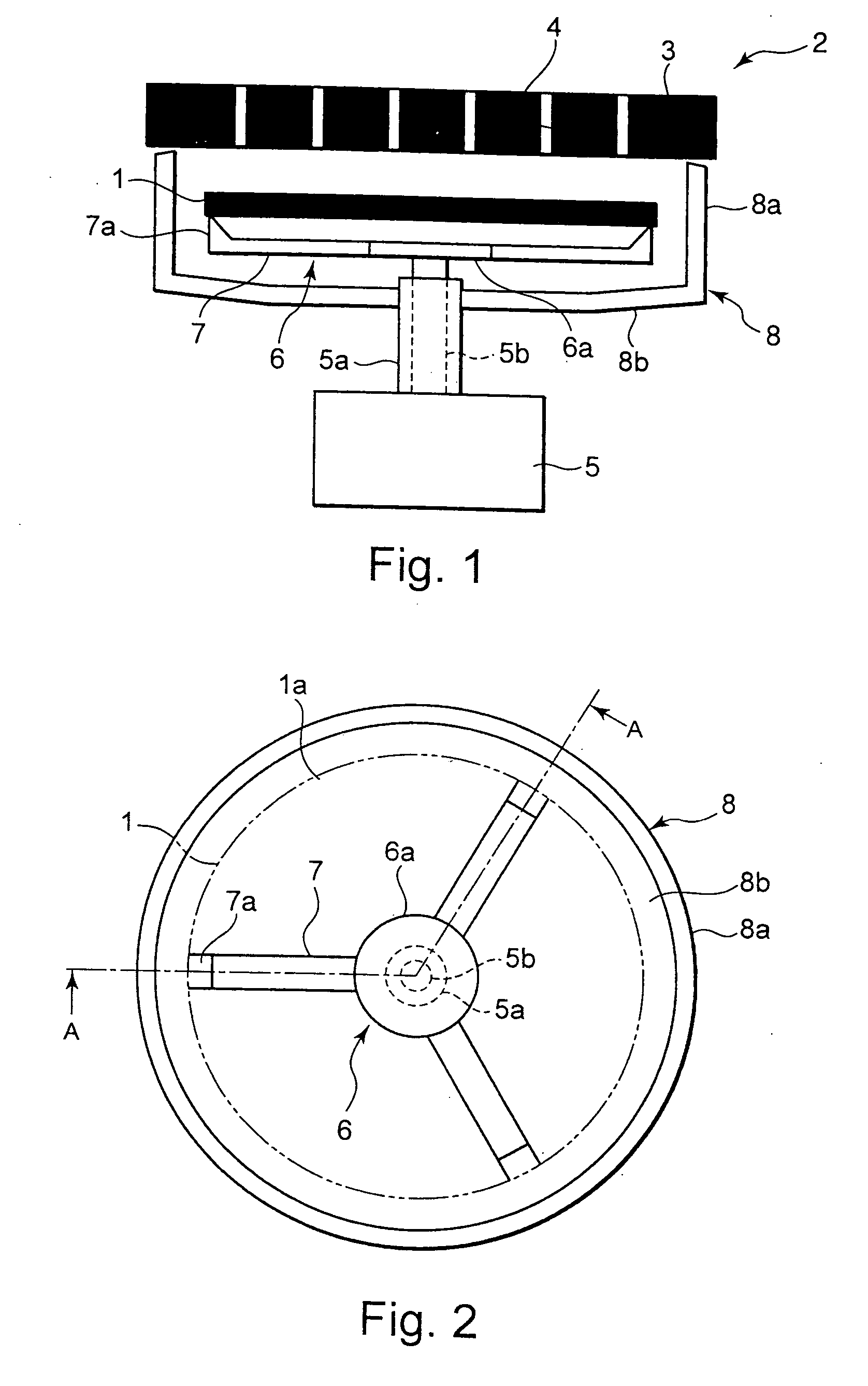
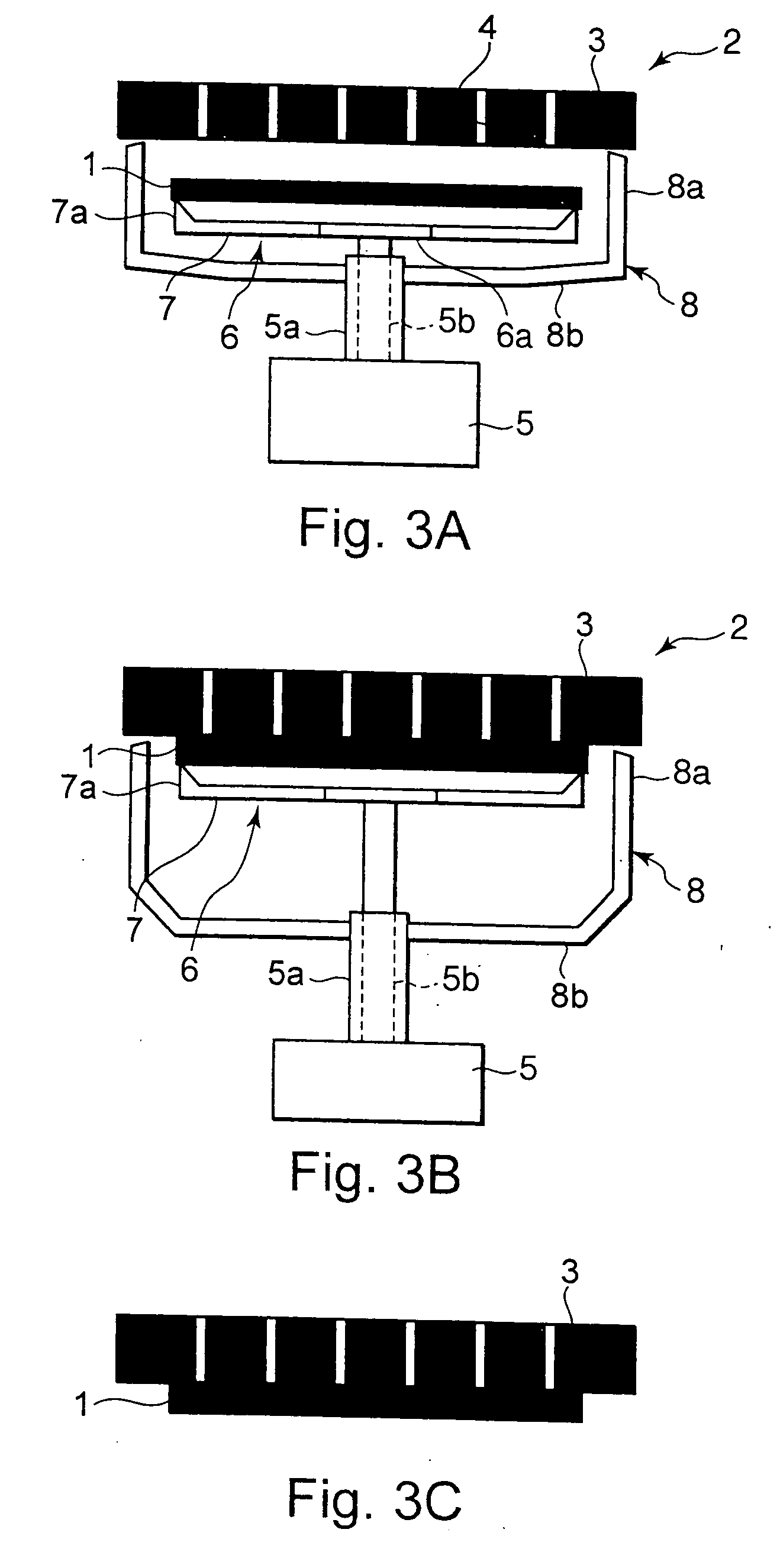
[0039]FIG. 1 is an explanatory view showing a section of a semiconductor manufacturing apparatus according to a first embodiment, and FIG. 2 is an explanatory view illustrating a top surface of the semiconductor manufacturing apparatus according to the first embodiment, respectively.

[0040] Incidentally, FIG. 1 shows a section taken along sectional line A-A shown in FIG. 2, and FIG. 2 is a top view showing a state in which a hot plate and a sapphire substrate shown in FIG. 1 are omitted. For elements similar to those shown in FIG. 10, the same reference numerals are given, and explanations thereof will be omitted.

[0041] In FIGS. 1 and 2, reference numeral 2 indicates the semiconductor manufacturing apparatus, which is a manufacturing apparatus such as an atmospheric-pressure CVD apparatus, which is employed in a process for manufacturing a semiconductor device while heating a sapphire substrate 1 or the like used as a substrate at a relatively low atmosphere temperature.

[0042] Ref...

second preferred embodiment

[0064]FIG. 4 is an explanatory view showing a section of a semiconductor manufacturing apparatus according to a second embodiment, and FIG. 5 is an explanatory view showing a top surface of the semiconductor manufacturing apparatus according to the second embodiment, respectively.

[0065] Incidentally, FIG. 4 shows a section taken along sectional line B-B shown in FIG. 5, and FIG. 5 is a top view showing a state in which the hot plate and sapphire substrate shown in FIG. 2 are excluded. For elements similar to those employed in the first embodiment, the same reference numerals are given and their explanations will be omitted.

[0066] In FIGS. 4 and 5, reference numeral 11 indicates a preheat plate, which is a disk-shaped member heated by an electric heater or the like and placed below a sapphire substrate 1 in opposition to its front surface. The preheat plate 11 is disposed on an upper surface of a support plate 6a so as to be spaced by a predetermined interval, e.g., an interval of ...

third preferred embodiment

[0078]FIG. 7 is an explanatory view showing a semiconductor manufacturing apparatus according to a third embodiment.

[0079] Incidentally, elements similar to those employed in the first and second embodiments are given the same reference numerals and their explanations will be omitted.

[0080] In FIG. 7, reference numeral 21 indicates a hot plate, which is heated by an electric heater or the like and heats a sapphire substrate 1 placed on its upper surface and which is used as a working table for process work in the corresponding process performed while heating the sapphire substrate 1.

[0081] Reference numeral 22 indicates a preheat plate, which is provided in the vicinity of the hot plate 21 and heated by an electric heater or the like, and which has the function of preheating the sapphire substrate 1 placed on its upper surface and lifting the sapphire substrate 1 from the upper surface by means of an unillustrated lift pin.

[0082] Reference numeral 23 indicates a transfer mechani...


PUM

PropertyMeasurementUnit
Temperatureaaaaaaaaaa
Lengthaaaaaaaaaa

Abstract

A semiconductor manufacturing apparatus A semiconductor manufacturing apparatus comprises a hot plate which heats a sapphire substrate; a support table having a support plate disposed with being spaced away from the hot plate by a predetermined interval, and support portions which respectively support the sapphire substrate with being spaced by a predetermined interval between the hot plate and the support plate and support the sapphire substrate in such a manner that back surfaces of the hot plate and the sapphire substrate are opposite to each other; an elevating device which moves the support table up and down; and a shielding cover which externally blocks off spacing defined between the hot plate and the sapphire substrate and spacing defined between the sapphire substrate and the support plate.

Description

BACKGROUND OF THE INVENTION [0001] The present invention relates to a semiconductor manufacturing apparatus employed in a process necessary to heat a sapphire substrate in a process for manufacturing a semiconductor device by the sapphire substrate or a sapphire wafer using the same, and a method for manufacturing the semiconductor device. [0002] A semiconductor device manufactured by a sapphire wafer in which silicon (Si) or the like has been epitaxially grown on a sapphire (Al2O3) substrate, is capable of greatly improving characteristics of a transistor by effects such as a reduction in parasitic capacitance, etc. as compared with a transistor of a semiconductor device manufactured by a silicon wafer using a silicon substrate. [0003] Generally, a process for manufacturing a semiconductor device using a sapphire wafer can substantially follow a process for manufacturing a semiconductor device using a silicon wafer. A semiconductor manufacturing apparatus is shared and its manufact...

Claims


Application Information

Patent Timeline
IPC IPC(8): H01L21/00
CPCH01L21/67103C23C16/481
Inventor YOSHIE, TORU
Owner LAPIS SEMICON CO LTD
Why Eureka
Try Eureka