Wiring board and method for manufacturing the same

a wiring board and wire technology, applied in the direction of conductive pattern formation, printed circuit non-printed electric components association, semiconductor/solid-state device details, etc., can solve the problems of generating warpage, small thickness and high density of wiring boards, and sometimes arising so as to achieve efficient suppression of warpage of wiring boards, reduce the effect of small thickness of wiring boards and reduced production costs

Inactive Publication Date: 2006-12-07
SHINKO ELECTRIC IND CO LTD
View PDF6 Cites 26 Cited by
  • Summary
  • Abstract
  • Description
  • Claims
  • Application Information

AI Technical Summary

Benefits of technology

[0045] Accordingly, the warpage of the wiring board can be efficiently suppressed.
[0046] According to the present invention, the small thickness of the wiring board in which the semiconductor chip is incorporated can be realized and warpage of the wiring board can be efficiently suppressed.

Problems solved by technology

However, when the small thickness and the high density of the chip incorporated wiring board are to be realized, a problem of warpage of the wiring board sometimes arises.
However, in such a laminated structure, a problem arises that the small thickness and the high density of the wiring board are hardly realized.
In recent years, since the semiconductor chips operating at high speed have a large quantity of heat generation, there is a problem that the wiring board in which the semiconductor chips are incorporated may possibly generate a warpage owing to the heat generation.
Especially, when the quantity of generated heat of the semiconductor chips is large, it is more difficult to reduce the warpage.

Method used


Image

  • Wiring board and method for manufacturing the same
  • Wiring board and method for manufacturing the same
  • Wiring board and method for manufacturing the same

Examples


first embodiment

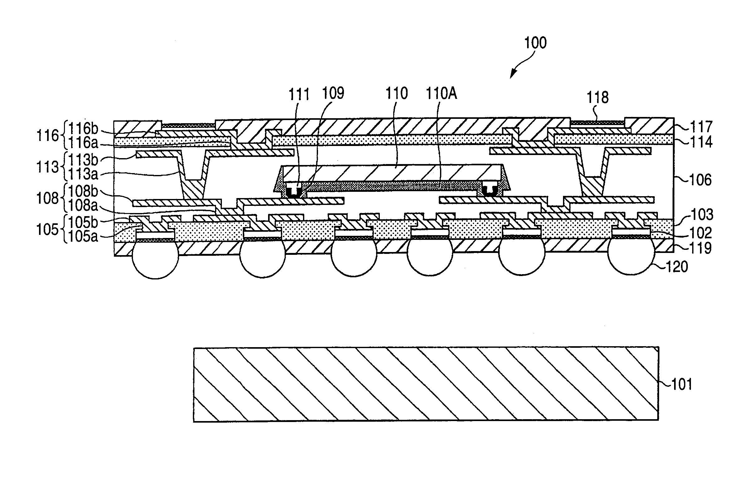
[0085]FIG. 1 is a sectional view schematically showing a wiring board 100 according to a first embodiment of the present invention. With reference to FIG. 1, the wiring board according to the present invention has an insulating layer 106 having a semiconductor chip 110 embedded and made of what is called a build-up resin material such as an epoxy. Reinforcing layers 103 and 114 for reinforcing the insulating layer 106 are respectively formed so as to come into contact with both the surfaces of the insulating layer 106.

[0086] The semiconductor chip 110 is connected to a wiring section (described below) and connected through the wiring section to an electrode 102 formed in the side of the reinforcing layer 103 (a lower side in the drawing, hereinafter) or an electrode 118 formed in the side of the reinforcing layer 114 (an upper side in the drawing, hereinafter). For instance, the electrode 102 or the electrode 118 is connected to a mother board or other devices, or connecting device...

second embodiment

[0137] The wiring board described in the first embodiment can be formed in a structure in which the warpage is more reduced as described below.

[0138]FIG. 3 is a sectional view schematically showing a wiring board 100A according to a second embodiment. In the drawing, the previously described parts are designated by the same reference numerals and an explanation thereof is omitted.

[0139] Referring to FIG. 3, in the wiring board 100A according to this embodiment, a reinforcing layer 121 that reinforces an insulating layer 106 is embedded in the insulating layer 106 and formed between a reinforcing layer 103 and a reinforcing layer 114.

[0140] Further, in the reinforcing layer 121, an opening portion 121A through which a via-plug 113a passes is formed. In such a way, the reinforcing layer is further added to the insulating layer 106 in addition to the structure shown in the first embodiment, so that the rigidity of the wiring board is more improved and an effect for suppressing the w...

third embodiment

[0143] In recent years, a problem arises that a semiconductor chip operating at high speed generates large quantity of heat so that a warpage is sometimes generated in a wiring board in which the semiconductor chip is incorporated.

[0144] Thus, when a heat radiating section for radiating the heat of the semiconductor chip is added to the wiring board shown in the first embodiment or the second embodiment, the damage of the semiconductor chip or an imperfect operation due to the generated heat is desirably reduced and the warpage of the wiring board due to the generated heat is reduced.

[0145]FIG. 4 is a sectional view schematically showing a wiring board 100B according to a third embodiment of the present invention. In the drawing, the previously described parts are designated by the same reference numerals and an explanation thereof is omitted.

[0146] Referring to FIG. 4, in the wiring board 100B according to this embodiment, a heat radiating section 200 is formed for radiating the...


PUM

PropertyMeasurementUnit
Young's modulusaaaaaaaaaa
thicknessaaaaaaaaaa

Abstract

A wiring board includes: a semiconductor chip; an insulating layer in which the semiconductor chip is embedded; a wiring connected to the semiconductor chip; and reinforcing layers for reinforcing the insulating layer, the reinforcing layers respectively formed on a front face side of the insulating layer and a rear face side of the insulating layer.

Description

[0001] This application claims foreign priority based on Japanese Patent application No. 2005-162547, filed Jun. 2, 2005, the content of which is incorporated herein by reference in its entirety. BACKGROUND OF THE INVENTION [0002] 1. Field of the Invention [0003] The present invention relates to a wiring board and a method for manufacturing the wiring board, and more particularly to a wiring board incorporating a semiconductor chip and a method for manufacturing the wiring board. [0004] 2. Description of the Related Art [0005] Nowadays, performances of electronic devices using semiconductor devices such as semiconductor chips have been progressively improved. A high density when the semiconductor chips are mounted on a board, the miniaturization of the board when the semiconductor chips are mounted and a saved space have been required. [0006] Accordingly, a board in which semiconductor chips are embedded, what is called a chip-incorporated wiring board has been proposed and various ...

Claims


Application Information

Patent Timeline
Patent Type & Authority Applications(United States)
IPC IPC(8): H05K1/00
CPCH01L23/3677Y10T29/4913H01L24/18H01L24/82H01L25/105H01L2221/68345H01L2224/16225H01L2224/18H01L2224/73204H01L2224/73253H01L2224/82039H01L2924/01015H01L2924/01029H01L2924/01033H01L2924/01075H01L2924/01078H01L2924/01079H01L2924/01082H01L2924/15311H05K1/0271H05K1/186H05K3/20H05K3/4644H05K3/4688H01L2924/01006H01L2924/01019H01L2924/01023H01L2924/01024H01L2924/014H01L2224/32225H01L23/5389Y10T29/49126Y10T29/49155Y10T29/49128H01L2225/1058H01L2225/1035H01L2924/3511H01L2924/00H01L2924/00012H01L21/568H01L24/19H01L2224/04105H01L2224/73259H01L2224/81005H01L2224/83005H01L2924/12042H01L2924/1533H01L2924/181H05K3/46
Inventor YAMANO, TAKAHARU
Owner SHINKO ELECTRIC IND CO LTD
Why Eureka
Try Eureka