Semiconductor devices having conductive pads and methods of fabricating the same

a technology of conductive pads and semiconductor devices, which is applied in the direction of semiconductor devices, semiconductor/solid-state device details, electrical apparatus, etc., can solve the problems of limiting the ability to highly integrate two-dimensional semiconductor memory devices, expensive apparatuses needed to form very fine micropatterns,

Active Publication Date: 2015-10-08
SAMSUNG ELECTRONICS CO LTD
View PDF2 Cites 390 Cited by
  • Summary
  • Abstract
  • Description
  • Claims
  • Application Information

AI Technical Summary

Problems solved by technology

Unfortunately, the apparatuses necessary to form very fine micropatterns may be expensive, which may limit the ability to highly integrate two-dimensional semiconductor memory devices.

Method used


Image

  • Semiconductor devices having conductive pads and methods of fabricating the same
  • Semiconductor devices having conductive pads and methods of fabricating the same
  • Semiconductor devices having conductive pads and methods of fabricating the same

Examples


Embodiment Construction

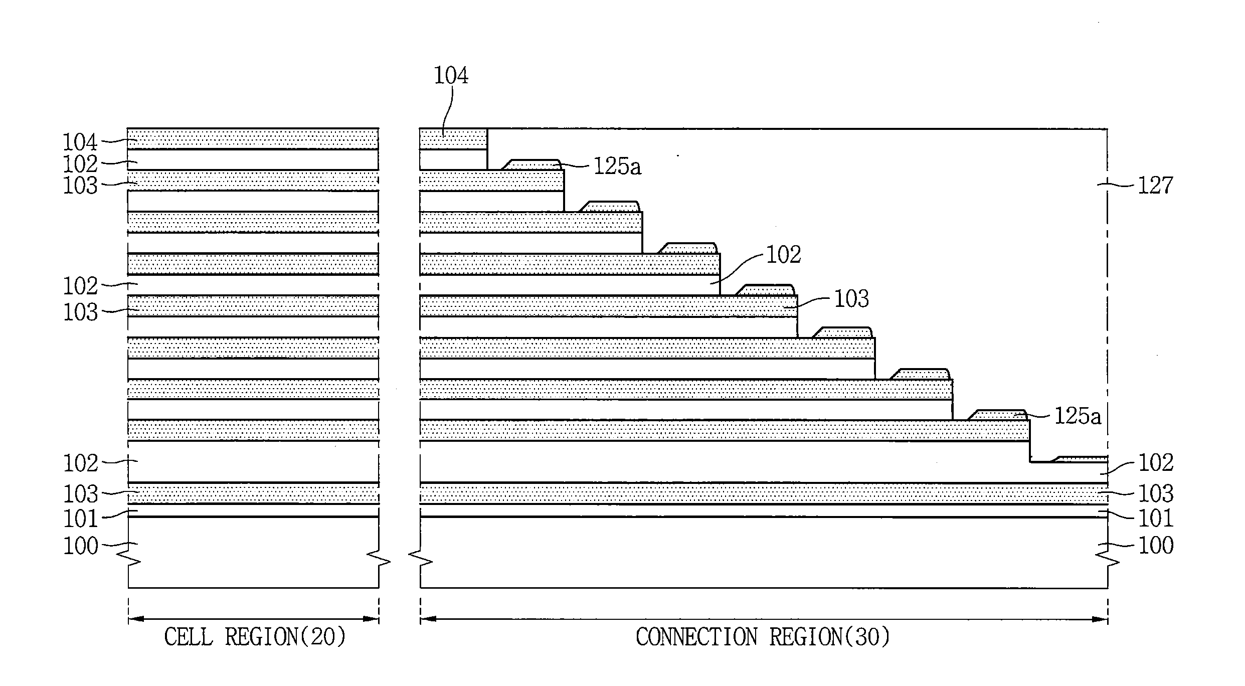
[0025]Various embodiments of the inventive concepts will now be described more fully with reference to the accompanying drawings in which some embodiments are shown. It will be appreciated, however, that the inventive concepts may be embodied in different forms and should not be construed as limited to the example embodiments set forth herein. Rather, these example embodiments are provided so that this disclosure is thorough and complete and fully conveys the inventive concepts to those skilled in the art.

[0026]The terminology used herein to describe embodiments of the inventive concepts is not intended to limit the scope thereof. The articles “a,”“an,” and “the” are singular in that they have a single referent; however, the use of the singular form in the present document should not preclude the presence of more than one referent. In other words, elements referred to in the singular form herein may number one or more, unless the context clearly indicates otherwise. It will be furth...


PUM


Abstract

A semiconductor device includes a substrate having a cell region and a connection region. A plurality of gate electrodes is stacked in a vertical direction in the cell region of the substrate. Conductive pads that are electrically connected to a peripheral circuit extend horizontally from the gate electrodes to the connection region. The conductive pads form a cascade structure in the connection region. Contact plugs that have different vertical lengths are electrically connected to respective ones of the conductive pads. The conductive pads have contact portions that are thicker in the vertical direction than the gate electrodes.

Description

CROSS-REFERENCE TO RELATED APPLICATION[0001]This application claims priority under 35 U.S.C. §119 to Korean Patent Application No. 10-2014-0041916, filed on Apr. 8, 2014, the disclosure of which is hereby incorporated by reference herein in its entirety.BACKGROUND[0002]1. Field[0003]Embodiments of the inventive concepts relate to semiconductor devices. More specifically, embodiments of the inventive concepts relate to semiconductor devices that include conductive pads having a portion that are thicker than corresponding gate electrodes, and to methods of fabricating such semiconductor devices.[0004]2. Description of Related Art[0005]Efforts are underway to further increase the integration density of semiconductor devices to improve their performance and / or to decrease the cost of manufacturing these devices. The integration density of a conventional two-dimensional memory device is determined by the area occupied by the unit memory cells of the device, and accordingly, may be influe...

Claims


Application Information

Patent Timeline
Patent Type & Authority Applications(United States)
IPC IPC(8): H01L27/02H01L23/522H01L23/495H01L27/105H01L23/528
CPCH01L27/0207H01L27/105H01L23/5226H01L23/49517H01L23/528H01L2924/0002H10B43/35H10B43/50H10B43/27H01L2924/00H01L29/7831
Inventor YUN, TAE-HWANPARK, JIN-TAEK
Owner SAMSUNG ELECTRONICS CO LTD
Why Eureka
Try Eureka