Method and apparatus for forming insulating film

a technology of insulating film and forming method, which is applied in the direction of electrical apparatus, basic electric elements, electric discharge tubes, etc., can solve the problems of difficult constant supply of hsub>2/sub>o, difficult to supply the same, and difficult to supply hsub>2/sub>o of certain purity, etc., to achieve clean and safe production, good insulating property, and high reliability

Inactive Publication Date: 2006-05-25
CANON KK
View PDF5 Cites 394 Cited by
  • Summary
  • Abstract
  • Description
  • Claims
  • Application Information

AI Technical Summary

Benefits of technology

[0014] In accordance with the present invention, it is enabled to provide a method and/or an apparatus for forming a silicon oxide film by oxidizing silicon through plasma, by which a large amount of OH radicals can be produced cleanly and safely and by which an insulating film having high reliability can be produced quickly. More specifically,

Problems solved by technology

In such case, however, it is not easy to supply a sufficient content of H2 into a reaction chamber and to produce a plenty of OH radicals.
However, regarding the gas gasified in accordance with the method described above, as compared with ordinary dry gases it is difficult to supply the same while controlling the flow rate stably.
Furthermore, it is difficult to supply H2O

Method used


Image

  • Method and apparatus for forming insulating film
  • Method and apparatus for forming insulating film
  • Method and apparatus for forming insulating film

Examples


example 1

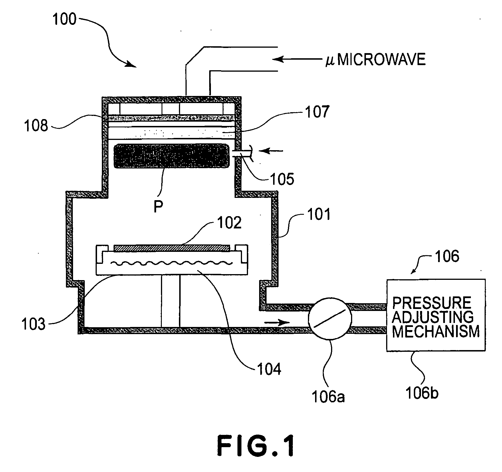
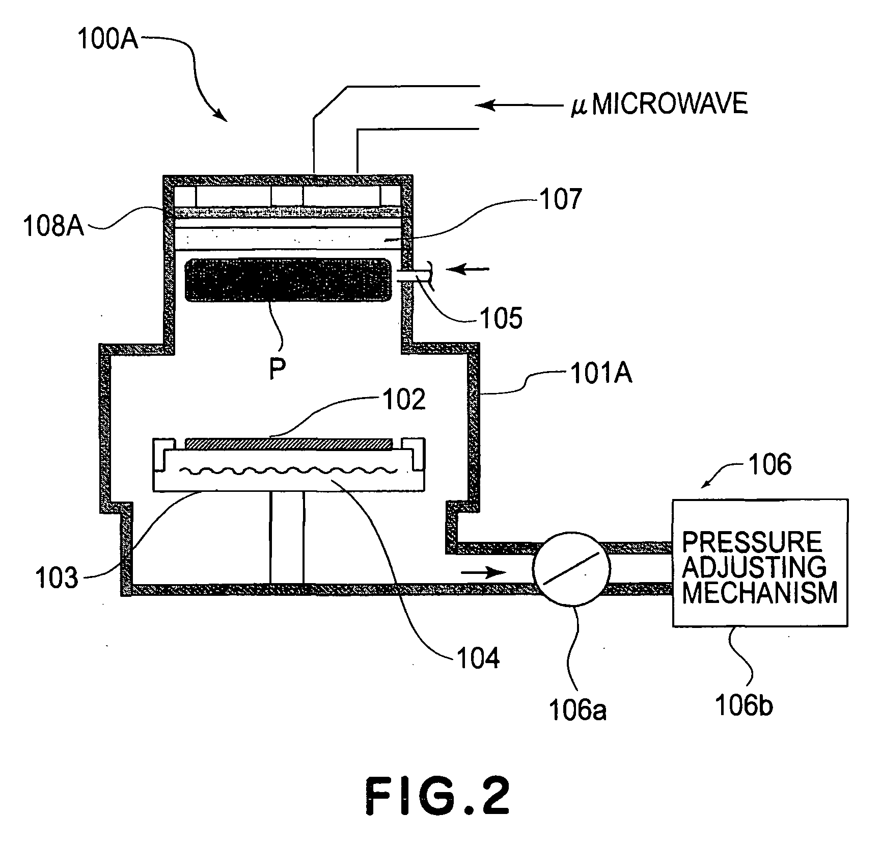
[0039] As an example of processing apparatus 100, a microwave plasma processing apparatus 100A shown in FIG. 2 was used to produce a gate insulating film for a semiconductor device. The processing apparatus 100A is arranged to cause excitement of surface wave interference plasma by microwaves. Denoted at 108A is a slotted endless circular waveguide (microwave supplying means) for introducing microwaves into a plasma processing chamber 101A through a dielectric material window 107. In FIG. 2, elements corresponding to those of FIG. 1 are denoted by corresponding reference numerals, while modified or specified elements are denoted by like numerals with an alphabetical suffix.

[0040] The slotted endless circular waveguide 108A had a TE10 mode and a sectional dimension of its inner wall of 27 mm×96 mm (guide wavelength 158.8 mm), and the center diameter of the waveguide was 151.6 mm (unit circumference is three times the guide wavelength). As regards the material of the waveguide 108A, ...

example 2

[0046] The microwave plasma processing apparatus 100A shown in FIG. 2 was used to produce a gate insulating film for a semiconductor device.

[0047] As regards the substrate 102 to be processed, an 8-inch P-type monocrystal silicon wafer (with a surface azimuth 100 and a specific resistance 10 Ωcm), having a polycrystal silicon film formed on its surface by a PECVC method, was used. First of all, the substrate 102 was conveyed into the plasma processing chamber 101, and it was placed on the support table 103. At that time, the substrate 102 was heated to and kept at 400° C. by means of the heater 104.

[0048] Subsequently, the processing chamber 101A was vacuum evacuated sufficiently by using a vacuum pump, to a vacuum level of 10−3 Pa. After that, an O2 gas, an NH3 gas and a He gas were introduced into the processing chamber, respectively, at flow rates of 200 sccm, 200 sccm and 600 sccm, respectively. The degree of opening of the pressure adjusting valve 106a was adjusted, and the i...

example 3

[0051] The microwave plasma processing apparatus 100A shown in FIG. 2 was used to perform corner rounding oxidation for STI (Shallow Trench Isolation).

[0052] As regards the substrate 102 to be processed, an 8-inch P-type monocrystal silicon wafer (with a surface azimuth 100 and a specific resistance 10 Ωcm), which was hard masked by Si3N4 and then etched to form an STI thereon, was used. First of all, the substrate 102 was conveyed into the plasma processing chamber 101, and it was placed on the support table 103. At that time, the substrate 102 was heated to and kept at 400° C. by means of the heater 104.

[0053] Subsequently, the processing chamber 101A was vacuum evacuated sufficiently by using a vacuum pump, to a vacuum level of 10−3 Pa. After that, an O2 gas, an NH3 gas and an Ar gas were introduced into the processing chamber, respectively, at flow rates of 1000 sccm, 200 sccm and 800 sccm, respectively. The degree of opening of the pressure adjusting valve 106a was adjusted, ...


PUM


Abstract

The present invention provides a method and apparatus for forming an insulating film having good reliability, in accordance with a process without high-temperature heating. In accordance with the present invention, in a process for forming an insulating film for a semiconductor device by oxidizing a material to be processed, exposed at the surface of a substrate to be processed, in accordance with plasma oxidation method, the plasma processing is carried out by use of at least a gas that contains hydrogen atoms other than H2 and H2O and a gas that contains oxygen atoms other than H2O.

Description

FIELD OF THE INVENTION AND RELATED ART [0001] This invention relates generally to a semiconductor device manufacturing process. More particularly, the invention concerns an insulating film forming method and apparatus for forming an oxide film upon the surface of a wafer through plasma processing. [0002] Conventionally, silicon dioxide films used as a gate insulating film of an MOS (Metal Oxide Semiconductor) type semiconductor device are produced in accordance with a oxidation method in which a silicon substrate is oxidized by heating it to a temperature of about 1000° C. in an oxidization ambience of dry oxygen or water vapor. With this method, however, an impurity layer already formed within the substrate may be re-diffused due to the heat, and the fineness may be prevented thereby. In consideration of this, a plasma oxidation method is becoming attractive because it can oxidize silicon at a lower temperature. In this plasma oxidation method, an oxidizing reaction gas is excited ...

Claims


Application Information

Patent Timeline
IPC IPC(8): H01L21/31H01L21/469
CPCH01J37/32192H01L21/02126H01L21/02236H01L21/02238H01L21/02252H01L21/31662
Inventor FUKUCHI, YUSUKE
Owner CANON KK
Why Eureka
Try Eureka