Display signal processing device and display device

a display signal and signal processing technology, applied in static indicating devices, non-linear optics, instruments, etc., can solve the problems of impaired color balance between red, green and blue, and difficulty in making the luminance of liquid crystal pixel proportional to the gradation value of display signals, so as to achieve the effect of increasing manufacturing costs

Active Publication Date: 2006-12-14
JAPAN DISPLAY INC
View PDF23 Cites 61 Cited by
  • Summary
  • Abstract
  • Description
  • Claims
  • Application Information

AI Technical Summary

Benefits of technology

[0012] The present invention has been made in consideration of the above-described problems, and an object of the invention is to provide a display signal processing device and display device that can convert a display signal to a gamma-corrected pixel voltage without considerably increasing manufacturing cost.

Problems solved by technology

In the above-described reference gradation voltage generating circuit, even if the resistance of the ladder resistor is tuned for gamma correction, it is difficult to make the luminance of the liquid crystal pixel proportional to the gradation value of the display signal.
Consequently, the color balance between red, green and blue is impaired when the luminance of each color is determined as a result of selection from a predetermined number of gradations including black and white.

Method used


Image

  • Display signal processing device and display device
  • Display signal processing device and display device
  • Display signal processing device and display device

Examples


first embodiment

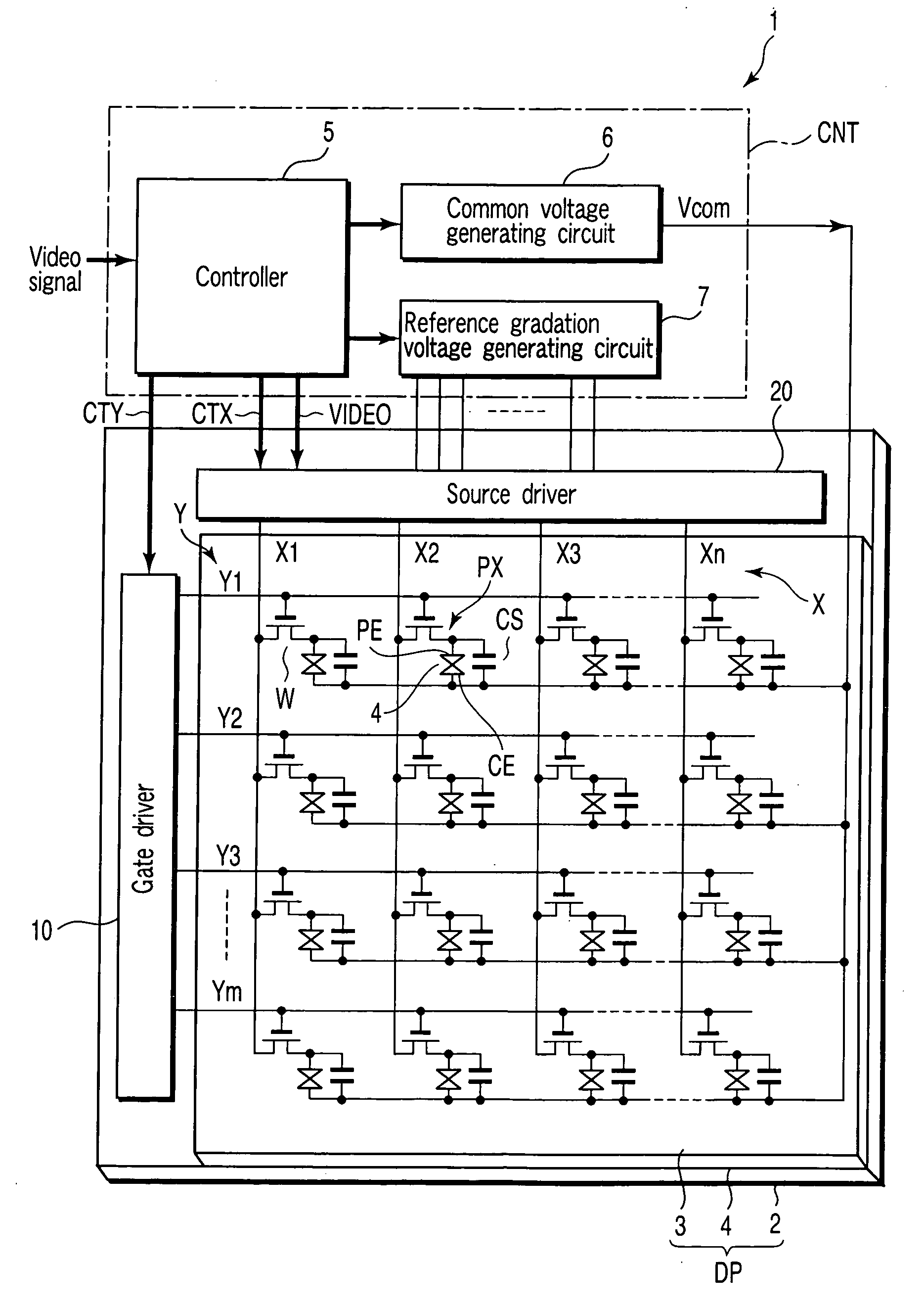
[0047] A liquid crystal display device according to the present invention, in which H / common inversion is executed, will now be described with reference to the accompanying drawings. FIG. 1 schematically shows the circuit configuration of the liquid crystal display device 1. The liquid crystal display device 1 includes a display panel DP providing an array of liquid crystal pixels PX, and a control unit CNT that controls the display panel DP. The display panel DP has a structure in which a liquid crystal layer 4 is held between an array substrate 2 and a counter-substrate 3.

[0048] The array substrate 2 includes a plurality of pixel electrodes PE that are arrayed in a matrix on a transparent insulating substrate such as a glass substrate; a plurality of gate lines Y (Y1 to Ym) that are arranged along the rows of pixel electrodes PE; a plurality of source lines X (X1 to Xn) that are arranged along the columns of pixel electrodes PE; pixel switching elements W that are arranged near in...

second embodiment

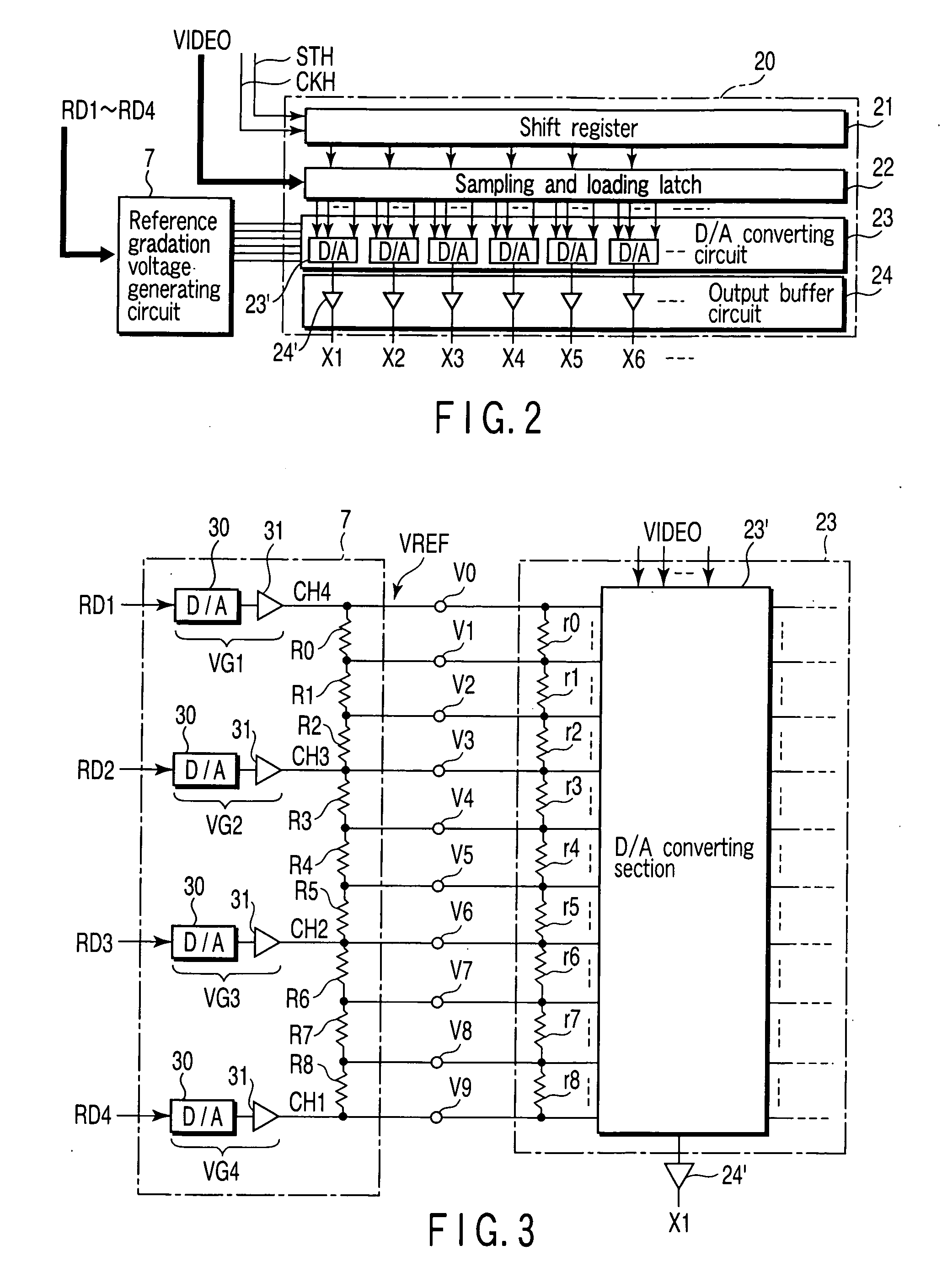
[0063] In the second embodiment, when an abnormal voltage occurs in any one of the variable voltage generating sections VG1 to VG4, the abnormal voltage is detected by an associated one of the four abnormal voltage detectors 32. As a result, the specified voltage VX is output from all the output terminals CH1 to CH4. Therefore, it is possible to avoid such a situation that the source driver 20 is destroyed by abnormal voltage that is output from the reference gradation voltage generating circuit 7 side.

[0064]FIG. 8 illustrates the operation of a first modification of the controller 5 shown in FIG. 1. In this modification, the controller 5 is configured to output the numeral data RD1 to RD4 to the reference gradation voltage generating circuit 7 in a specified order. As is shown in FIG. 8, the D / A conversion periods for the numeral data RD1 to RD4 are different from each other. In a certain frame, the potential of the output terminal CH4 of the variable voltage generating section VG1...


PUM

PropertyMeasurementUnit
voltageaaaaaaaaaa
voltageaaaaaaaaaa
voltageaaaaaaaaaa

Abstract

A display signal processing device includes a reference gradation voltage generating circuit that generates ten reference gradation voltages, and a D/A converting circuit that converts a video signal to a pixel voltage by selectively using the ten reference gradation voltages obtained from the reference gradation voltage generating circuit. The reference gradation voltage generating circuit includes four variable voltage generating sections that generate output voltages, which are varied for gamma correction, and nine resistors that are connected to divide difference voltages obtained between output terminals of the four variable voltage generating sections into the ten reference gradation voltages.

Description

CROSS-REFERENCE TO RELATED APPLICATIONS [0001] This is a Continuation Application of PCT Application No. PCT / JP2005 / 002932, filed Feb. 23, 2005, which was published under PCT Article 21(2) in Japanese.[0002] This application is based upon and claims the benefit of priority from prior Japanese Patent Application No. 2004-046898, filed Feb. 23, 2004, the entire contents of which are incorporated herein by reference. BACKGROUND OF THE INVENTION [0003] 1. Field of the Invention [0004] The present invention relates generally to display signal processing and display devices for converting a display signal to a pixel voltage, and more particularly to display signal processing and display devices for converting a display signal to a gamma-corrected pixel voltage. [0005] 2. Description of the Related Art [0006] A flat-panel display device, which is represented by a liquid crystal display device, is widely used as a display device for a personal computer, a mobile information terminal, a TV, ...

Claims


Application Information

Patent Timeline
Patent Type & Authority Applications(United States)
IPC IPC(8): G09G3/36G02F1/133G09G3/20
CPCG09G3/3611G09G3/3696G09G2310/027G09G2330/04G09G2320/0606G09G2320/0673G09G2320/0233G02F1/133G09G3/20G09G3/36
Inventor KANEDA, HARUTOSHISHIGEHIRO, KOJI
Owner JAPAN DISPLAY INC
Why Eureka
Try Eureka