Method for testing a hall magnetic field sensor on a wafer

a hall magnetic field and sensor technology, applied in the direction of voltage/current isolation, measurement devices, instruments, etc., can solve the problems of complicated mechanical system, increased hardware cost, and increased cost of the test equipment,

Inactive Publication Date: 2006-12-21
TDK MICRONAS GMBH
View PDF8 Cites 0 Cited by
  • Summary
  • Abstract
  • Description
  • Claims
  • Application Information

AI Technical Summary

Benefits of technology

[0013] A wafer or Hall sensor with an evaluation circuit in the signal pathway of the Hall plate, wherein the determined electrical resistance also detects the influence of the evaluation circuit. The evaluation circuit in the signal pathway of the Hall plate enables testing of the evaluation circuit by an applied Hall current. In this way, it is also possible to check the further signal pathway by generating a signal, such as would also be generated by a magnetic field.

Problems solved by technology

Generating precise magnetic fields suitable for a test with commercially available mixed-signal testing systems is not possible without additional devices, so an additional and undesirable hardware expense is incurred.
Since different magnetic field strengths are usually needed for a test, one must expect relatively long transient times for the coils producing them, or a complicated mechanical system.
In addition, because the homogeneous region of the magnetic field produced in this way is relatively small, only a few sensors can be tested at the same time on a wafer.
Since a Helmholtz layout is not possible for the coils producing such a magnetic field for a wafer test with a thermochuck, one can only provide an inexact magnetic field for the testing or sampling.
Currents flow in the thermochuck, generating disruptive magnetic fields.
In particular, for a Helmholtz layout one would require a coil in the thermochuck, which would be difficult to implement, so that in the final analysis there are many problems with magnetic measurements of a wafer in conjunction with a thermochuck.

Method used


Image

  • Method for testing a hall magnetic field sensor on a wafer
  • Method for testing a hall magnetic field sensor on a wafer

Examples


Embodiment Construction

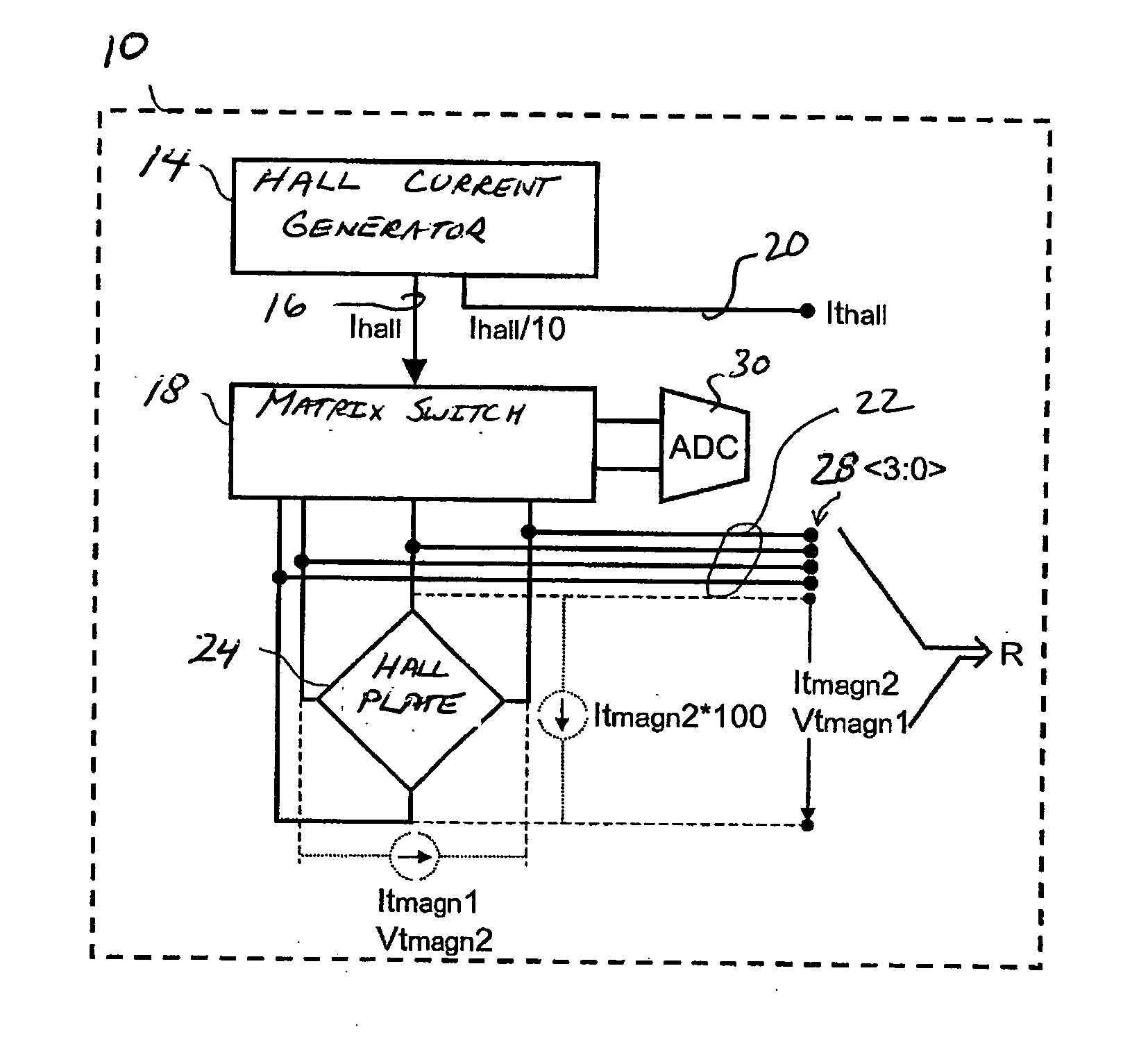
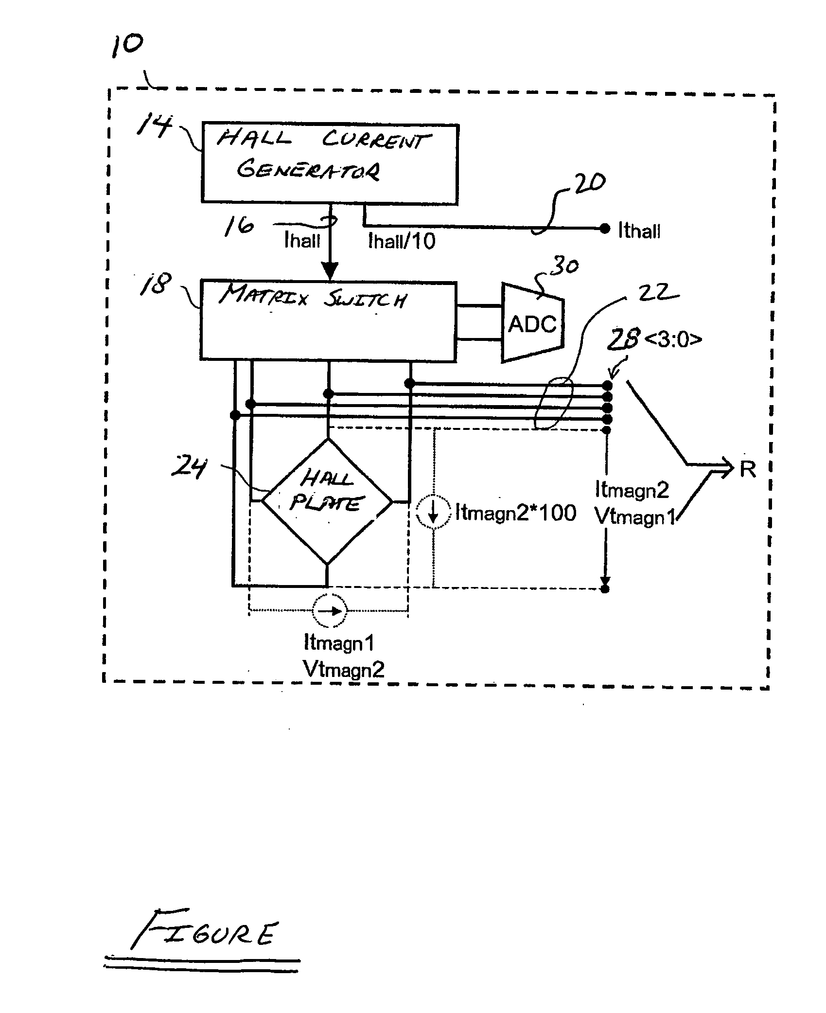
[0018] The FIGURE illustrates a block diagram illustration of a layout of components on a wafer or a corresponding Hall sensor configured in such a way that a metering current may be applied to check individual components, and especially the components of a signal pathway with respect to their electrical resistance R. From the electrical resistance the quality of the investigated segment can be determined, without having to apply an external magnetic field. One application which is advantageous is integrated Hall sensors with evaluation circuits.

[0019] A portion of a wafer 10 is shown for configuring an integrated circuit sensor. A reference current from a bias generator is input to a Hall current generator 14. Thus, the currents are generated in the bias generator, which provides reference currents and reference voltages for practically all the analog circuits on the sensor. The Hall current generator 14 outputs a Hall current as a metering current Ihall on a line 16 to a matrix s...


PUM


Abstract

A method for testing a Hall magnetic field sensor on a wafer includes generating a current flow in a Hall plate of the Hall magnetic field sensor. At least one voltage value across first and second nodes is measured and a measured voltage signal is provided indicative thereof. An electrical resistance based upon the measured voltage and the current is then determined, in the absence of an applied test magnet field.

Description

PRIORITY INFORMATION [0001] This patent application claims priority from German patent application 10 2005 028 461.2 filed Jun. 17, 2005, which is hereby incorporated by reference. BACKGROUND OF THE INVENTION [0002] The invention relates to testing a semiconductor wafer, and in particular to testing a Hall magnetic field sensor. [0003] Magnetic fields are used for testing of semiconductor wafers, especially Hall magnetic field sensors, during a production test as part of the manufacturing process. Generating precise magnetic fields suitable for a test with commercially available mixed-signal testing systems is not possible without additional devices, so an additional and undesirable hardware expense is incurred. Since different magnetic field strengths are usually needed for a test, one must expect relatively long transient times for the coils producing them, or a complicated mechanical system. In addition, because the homogeneous region of the magnetic field produced in this way is...

Claims


Application Information

Patent Timeline
Patent Type & Authority Applications(United States)
IPC IPC(8): G01R33/07
CPCG01R31/2831G01R31/2829
Inventor BIDENBACH, REINERSCHUBERT, JENSKREDLER, STEFANJANKE, RALF
Owner TDK MICRONAS GMBH
Why Eureka
Try Eureka