Multi-chip device and method for producing a multi-chip device

Inactive Publication Date: 2006-12-21
POLARIS INNOVATIONS
View PDF2 Cites 39 Cited by
  • Summary
  • Abstract
  • Description
  • Claims
  • Application Information

AI Technical Summary

Benefits of technology

[0010] One embodiment of the present invention provides a multi-chip device with stacked memory chips which is designed to be manufactured with an increased yield and which allows an increa

Problems solved by technology

In practice, however, the rate of increase in capacity dictated by the market is not achievable.
Consequently, there is a technological gap which is nowadays filled by stacking memory chips onto each other to provide sufficient memory capacity on a memory module.
One problem with manufacturin

Method used


Image

  • Multi-chip device and method for producing a multi-chip device
  • Multi-chip device and method for producing a multi-chip device
  • Multi-chip device and method for producing a multi-chip device

Examples


Example

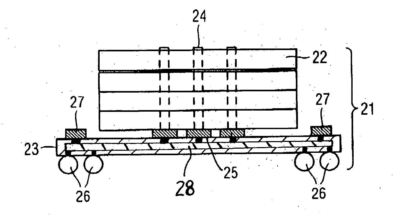
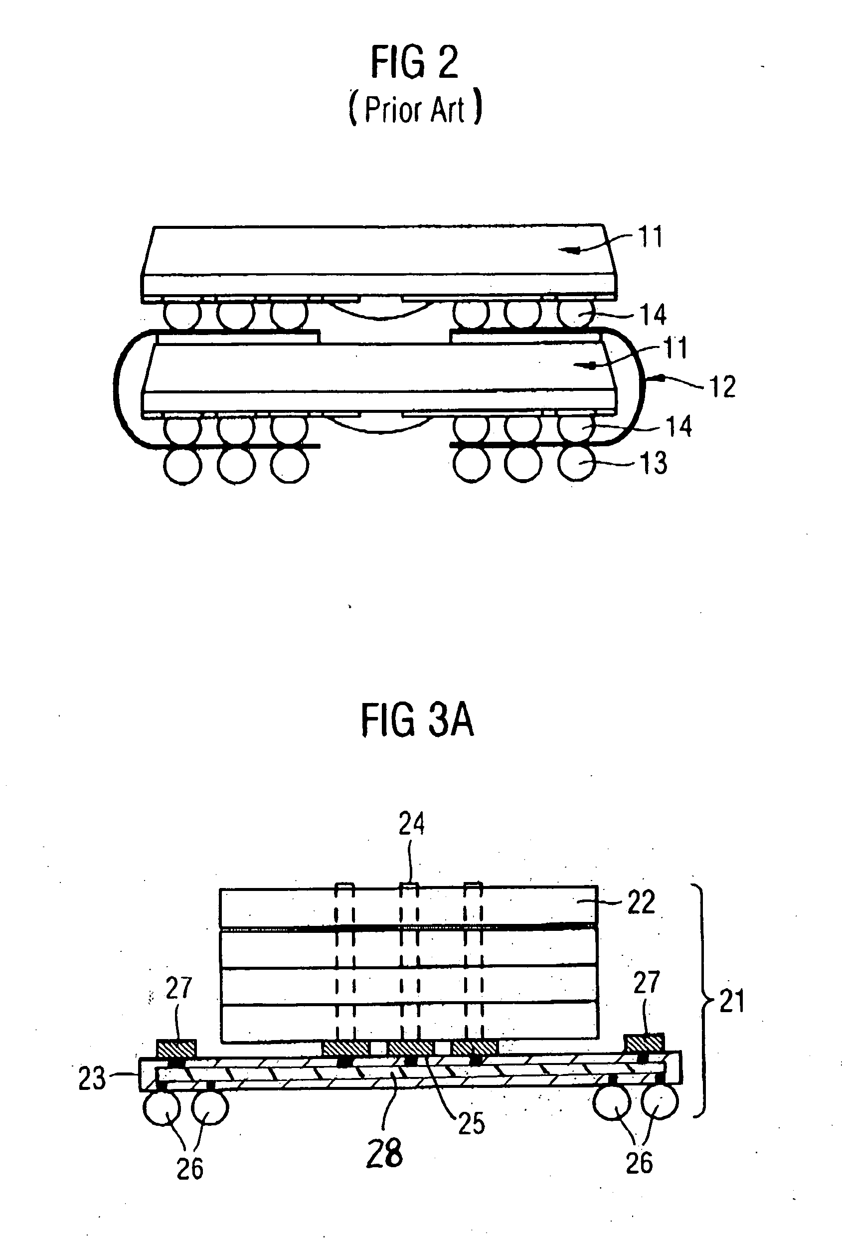
[0020] In the following, reference is made to embodiments of the invention. However, it should be understood that the invention is not limited to specific described embodiments. Instead, any combination of the following features and elements, whether related to different embodiments or not, is contemplated to implement and practice the invention. Furthermore, in various embodiments the invention provides numerous advantages over the prior art. However, although embodiments of the invention may achieve advantages over other possible solutions and / or over the prior art, whether or not a particular advantage is achieved by a given embodiment is not limiting of the invention. Thus, the following aspects, features, embodiments and advantages are merely illustrative and are not considered elements or limitations of the appended claims except where explicitly recited in a claim(s). Likewise, reference to “the invention” shall not be construed as a generalization of any inventive subject ma...


PUM


Abstract

The present invention relates to a multi-chip device comprising a plurality of chip stacks each including a plurality of single chips stacked on each other, wherein the stacked single chips are electrically interconnected by one or more through-chip-connection extending through at least one of the single chips and a substrate providing one or more first contact elements each of which is in contact with one of the through-chip-connections and providing one or more second contact elements being in electrical contact with the first contact elements, wherein the plurality of chip stacks are stacked onto each other and wherein the second contact elements of one of the chip stacks each being arranged to be in contact to one or more third contact elements of an adjacent one of the chip stacks.

Description

BACKGROUND OF THE INVENTION [0001] 1. Field of the Invention [0002] The present invention relates to a multi-chip device including a plurality of chips. The present invention further relates to a method for producing a multi-chip device comprising a plurality of chips. [0003] 2. Description of the Related Art [0004] Market requirements demand constantly increasing storage capacity of memory modules. In practice, however, the rate of increase in capacity dictated by the market is not achievable. Consequently, there is a technological gap which is nowadays filled by stacking memory chips onto each other to provide sufficient memory capacity on a memory module. [0005] A number of stacking technologies are known. In one stacking technique, a two or more memory chips are stacked upon each other, each chip being separated by a spacer. Each of the memory chips is separately wire-bonded onto a common substrate which provides an electrical redistribution to, e.g., solder balls and the like b...

Claims


Application Information

Patent Timeline
IPC IPC(8): H05K1/00
CPCH01L25/0657H01L25/105H01L2224/73265H01L2224/32225H01L2225/1094H01L2225/1058H01L2225/1023H01L2924/15311H01L2924/14H01L2225/06589H01L2225/06572H01L2225/06551H01L2225/06541H01L2225/0652H01L2225/06513H01L2224/48091H01L2224/48227H01L2224/48471H01L2924/00014H01L2924/00
Inventor THOMAS, JOCHENSCHOENFELD, OLAF
Owner POLARIS INNOVATIONS
Why Eureka
Try Eureka