Substrate processing system and substrate processing method

Inactive Publication Date: 2006-12-21
TOKYO ELECTRON LTD
View PDF11 Cites 2 Cited by
  • Summary
  • Abstract
  • Description
  • Claims
  • Application Information

AI Technical Summary

Benefits of technology

[0024] The present invention has been made in view of the foregoing circumstances and it is an object of the present invention to provide a substrate processing system including first and second systems in combination for processing a plurality of substrates by a single-wafer processing method by the cooperation of the first and the second system and capable of restricting incase in cost and footprints and decrease in yield and throughput, and to provide a substrate processing method to be carried out by the same substrate processing system.

Problems solved by technology

If the resist film forming and developing system and the exposure system do not cooperate properly, the improper cooperation of the resist film forming and developing system and the exposure system affects the width of lines of a pattern adversely and reduces yield.
A conventional method of cooperation is very likely to cause the foregoing problems.
For example, the in-line process to be carried out by the resist film forming and developing system 200 and the exposure system 201 shown in FIG. 9 has a problem that it takes an excessively long time for changing process conditions for some one of the process jobs.
Wafers cannot be processed for a process temperature setting operation for setting the process temperature.
However, the hardware increases the cost of the resist film forming and developing system 200 and increases footprints.

Method used


Image

  • Substrate processing system and substrate processing method
  • Substrate processing system and substrate processing method
  • Substrate processing system and substrate processing method

Examples


Embodiment Construction

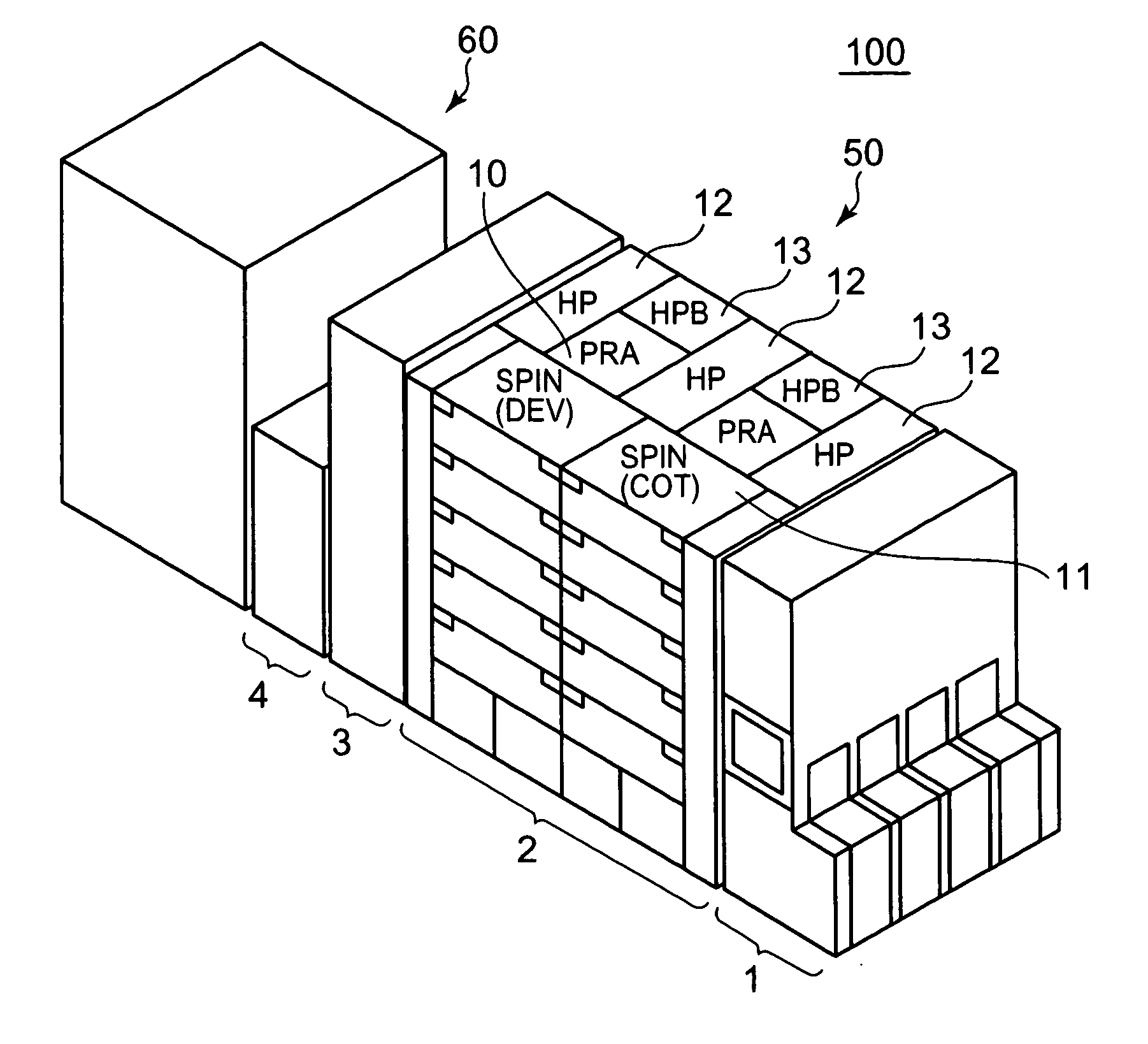
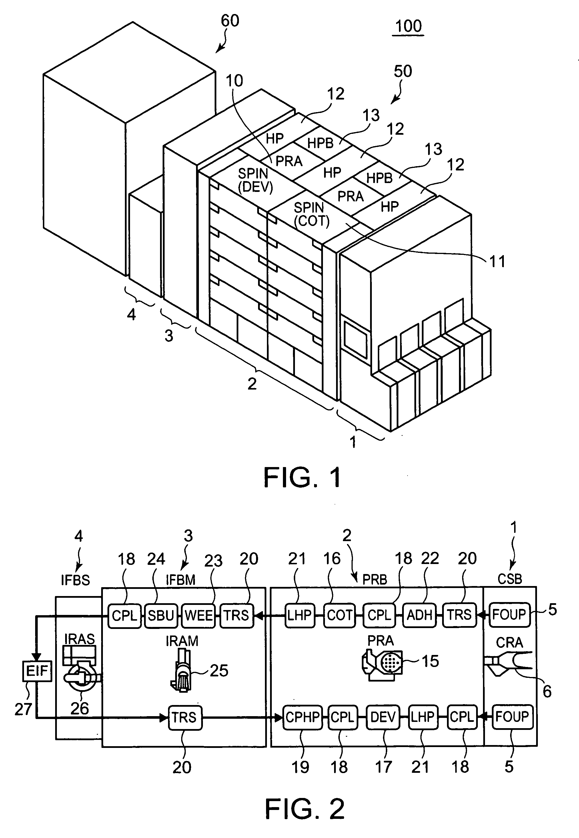
[0061] A substrate processing system and a substrate processing methods of the present invention will be described in terms of preferred embodiments thereof shown in the accompanying drawings. FIG. 1 is a perspective view of a pattern forming system 100, namely, a substrate processing system, in a preferred embodiment according to the present invention and FIG. 2 is a diagrammatic view showing sequential steps of a process to be carried out by the pattern forming system shown in FIG. 1.

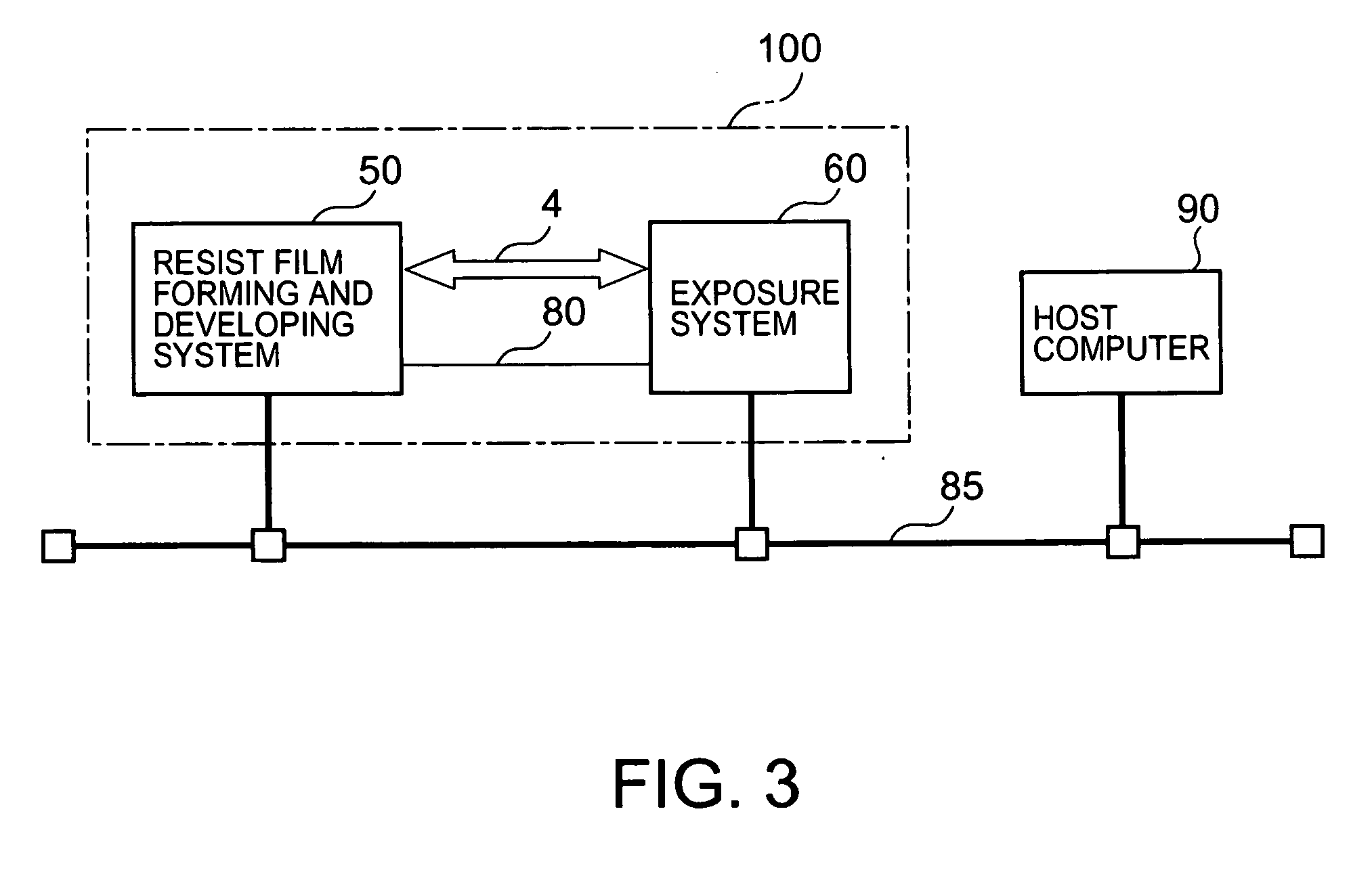
[0062] The pattern forming system 100 shown in FIG. 1 is used in a photolithographic process in an electronic device manufacturing process for manufacturing electronic devices, such as semiconductor devices or liquid crystal displays. The pattern forming system 100 includes a resist film forming and developing system (first processing system) 50 and an exposure system (second processing system) 60. The resist film forming and developing system 50 and the exposure system 60 are connected to carry out ...


PUM

PropertyMeasurementUnit
Timeaaaaaaaaaa

Abstract

A substrate processing system 100 and a substrate processing method process a plurality of substrates in a single-substrate processing mode by the cooperative operation of a first processing system and a second processing system. The substrate processing system 100 suppresses increase in cost and footprint and the reduction of yield and throughput. The substrate processing system 100 includes a first processing system 50 for processing substrates in a single-substrate processing mode and a second processing system 60 for processing substrates in a single-substrate processing mode. The second processing system 60 processes a substrate processed by a first process by the first processing system 50 by a second process, and the first processing system processes the substrate processed by the second process by the second processing system 60 by a third process. The first processing system 50 includes a first control means 30 for controlling a substrate carrying operation. The second processing system 60 includes a second control means 40. The first control means 30 (or the second control means 40) obtains information about processing time needed by the second processing system 60 (the first processing system 50) and controls a substrate carrying operation for carrying substrates between the first processing system 50 and the second processing system 60 on the basis of the obtained information.

Description

BACKGROUND OF THE INVENTION [0001] 1. Field of the Invention [0002] The present invention relates to a substrate processing system and a substrate processing method for processing a plurality of substrates on an in-line system including a plurality of processing apparatuses in a single-substrate processing mode. [0003] 2. Description of the Related Art [0004] In a photolithographic process included in an electronic device manufacturing process for manufacturing an electronic device, such as a semiconductor device, a resist film forming and developing apparatus for applying a liquid resist (hereinafter, referred to simply as “resist”) to a substrate, such as a wafer, in a resist film and processing the resist film by a developing process, and an exposure unit for processing the substrate coated with the resist film by an exposure process are used in combination to achieve an in-line processing operation. [0005] Referring to FIG. 9 typically showing a substrate processing system, a re...

Claims


Application Information

Patent Timeline
IPC IPC(8): C04B35/45H01L21/027
CPCG03F7/70533G03F7/7075H01L21/67155H01L21/67276H01L21/67184H01L21/67196H01L21/67253H01L21/67173G03F7/70508
Inventor KANEKO, TOMOHIROMIYATA
Owner TOKYO ELECTRON LTD
Why Eureka
Try Eureka