
Finfets, nonvolatile memory devices including finfets, and methods of forming the same

a nonvolatile memory and finfet technology, applied in the field of semiconductor devices, can solve the problems of increasing the difficulty of manufacturing transistors having a general horizontal channel structure, the inability to scale down horizontal channel structure transistors, and the short channel effect, so as to reduce the width of the fins

Active Publication Date: 2006-12-28
SAMSUNG ELECTRONICS CO LTD
View PDF23 Cites 88 Cited by
  • Summary
  • Abstract
  • Description
  • Claims
  • Application Information

AI Technical Summary

Benefits of technology

The present invention provides a fin field effect transistor (FinFET) and related nonvolatile memory devices that can reduce program disturbances and improve isolation between fins. The invention includes an insulating layer between the fins and the substrate to improve isolation. The insulating layer has a different thickness than the device isolation layer, which helps to prevent program disturbances. The FinFET also includes a fin that extends away from the substrate and is surrounded by a device isolation layer and a tunnel insulating layer. A blocking insulating layer is formed on the fin to prevent program disturbances. The invention also provides a method of forming the FinFET and the nonvolatile memory devices. The invention can be used in highly integrated semiconductor devices and is cost-effective.

Problems solved by technology

As device feature sizes and associated design rules continue to be driven smaller, transistors having a general horizontal channel structure are increasingly more difficult to manufacture.
There appears to be some limitations to the ability to scale down horizontal channel structure transistors.
One potentially serious limitation is a short channel effect and a drain induced barrier lower (DIBL) effect, which can occur more often as the channel length is shortened.
Moreover, if the channel length is reduced to 30 nm or less, it is known to be more difficult for a transistor to exhibit desired operational characteristics because of strong short channel effects and DIBL effects.
As a result, the gate electrode may not effectively control the transistor between ON / OFF states, and short channel effects due to the reduction of the channel length can become a serious problem.
Resultingly, there may occur a program disturbance by which the second cell transistor TR2 is undesirably programmed.
However, the thickness of the device isolation layer 102 is restricted by the height of the fin 101.
However, SOI substrate processes can be very expensive and a back bias may not be applied thereto.

Method used


Image

  • Finfets, nonvolatile memory devices including finfets, and methods of forming the same
  • Finfets, nonvolatile memory devices including finfets, and methods of forming the same
  • Finfets, nonvolatile memory devices including finfets, and methods of forming the same

Examples


Embodiment Construction

[0009] Some embodiments of the present invention provide a fin field effect transistor (FET) and related nonvolatile memory devices which may be capable of reducing the occurrence of or preventing program disturbances.

[0010] Some other embodiments of the present invention provide a method of forming a nonvolatile memory device using a FinFET that may be capable of reducing the occurrence of or preventing program disturbances.

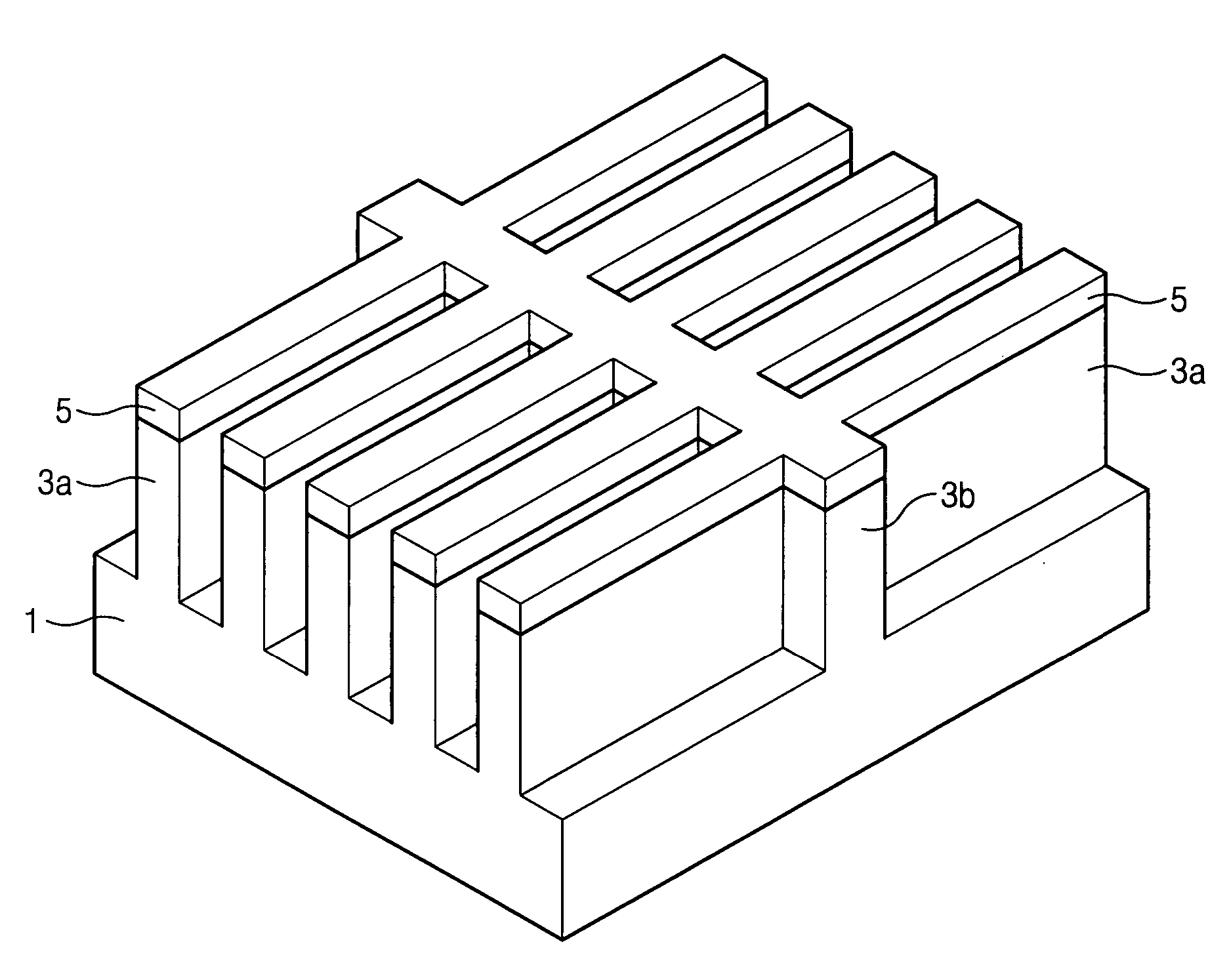
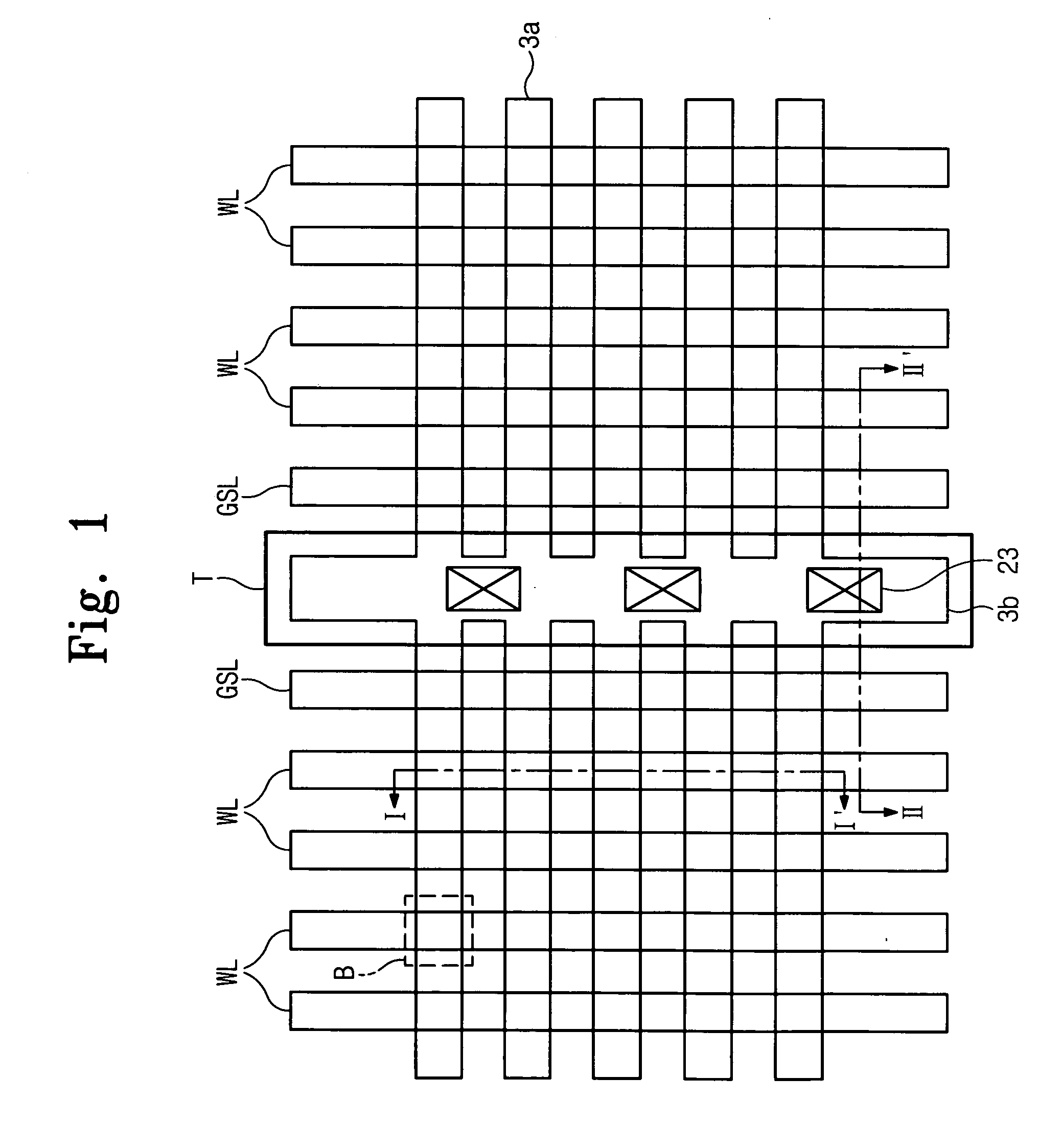
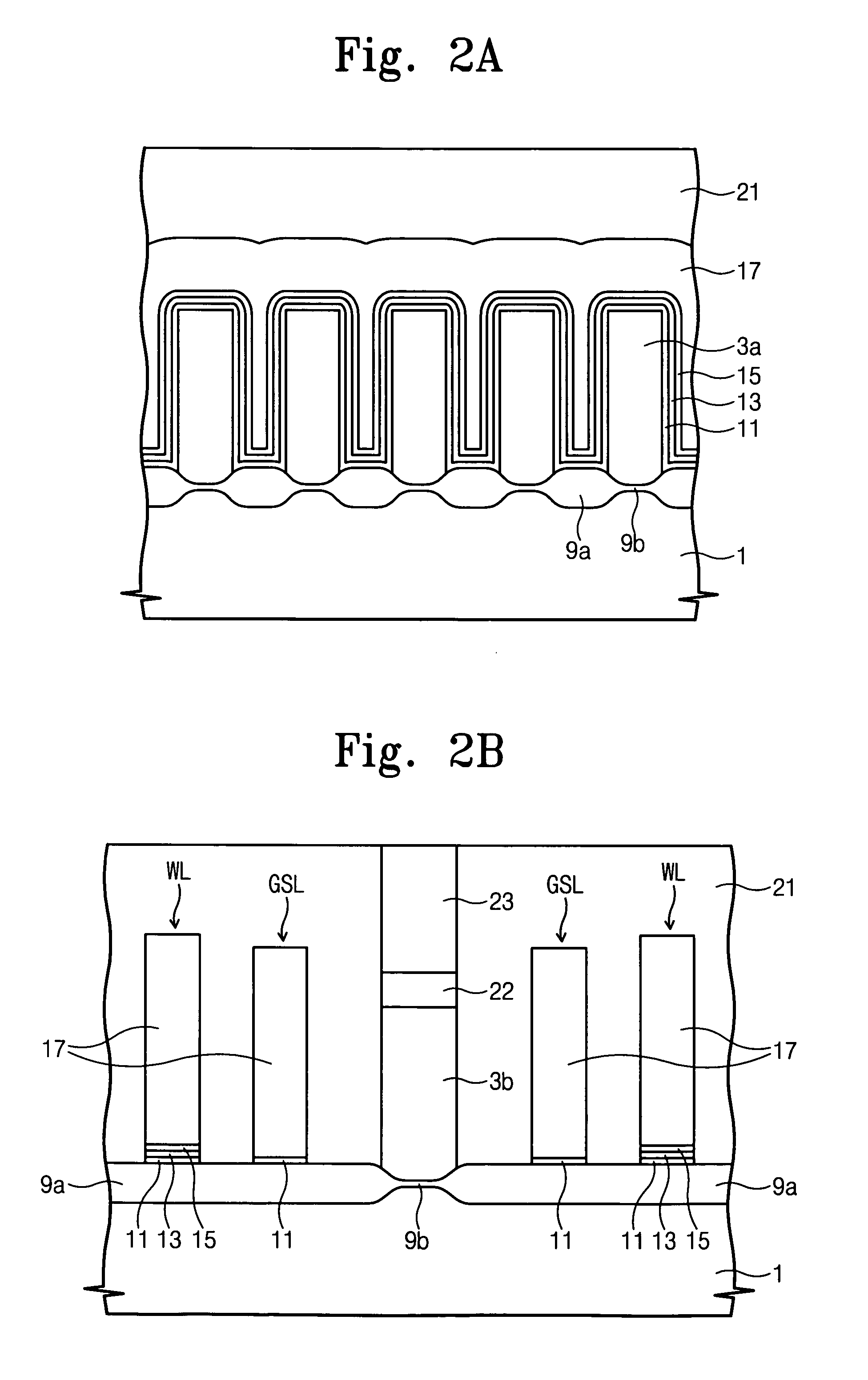
[0011] In accordance with some embodiments, the FinFETs include an insulating layer between their fins and a substrate to improve the isolation of the fins from one another.

[0012] In some embodiments, a FinFET includes a fin that is on a substrate and extends away from the substrate. A device isolation layer is disposed on the substrate on both sides of the fin. An insulating layer is between the fin and the substrate. The insulating layer is directly connected to the device isolation layer and has a different thickness than the device isolation layer. A gate...


PUM


Abstract

A FinFET includes a fin that is on a substrate and extends away from the substrate. A device isolation layer is disposed on the substrate on both sides of the fin. An insulating layer is between the fin and the substrate. The insulating layer is directly connected to the device isolation layer and has a different thickness than the device isolation layer. A gate electrode crosses over the fin. A gate insulating layer is between the gate electrode and the fin. Source and drain regions are on the fins and on opposite sides of the gate electrode. Related nonvolatile memory devices that include FinFETs and methods of making FinFETs and nonvolatile memory devices are also disclosed.

Description

CROSS REFERENCE TO RELATED APPLICATION [0001] This application claims priority under 35 USC § 119 to Korean Patent Application No. 10-2005-0054688 filed on Jun. 23, 2005, the content of which is incorporated herein by reference in its entirety. FIELD OF THE INVENTION [0002] The present invention relates to semiconductor devices and methods of forming the same, and more particularly, to fin field effect transistors (FinFETs) and nonvolatile memory devices using FinFETs, and methods of forming the same. BACKGROUND OF THE INVENTION [0003] As device feature sizes and associated design rules continue to be driven smaller, transistors having a general horizontal channel structure are increasingly more difficult to manufacture. There appears to be some limitations to the ability to scale down horizontal channel structure transistors. One potentially serious limitation is a short channel effect and a drain induced barrier lower (DIBL) effect, which can occur more often as the channel length...

Claims


Application Information

Patent Timeline
Patent Type & Authority Applications(United States)
IPC IPC(8): H01L21/8234H01L29/94H10B69/00
CPCH01L21/28282H01L27/115H01L27/11568H01L29/42332H01L29/792H01L29/66833H01L29/785H01L29/7881H01L29/66795H01L29/40117H10B43/30H10B69/00
Inventor LEE, CHANG-HYUN
Owner SAMSUNG ELECTRONICS CO LTD
Features
  • Generate Ideas
  • Intellectual Property
  • Life Sciences
  • Materials
  • Tech Scout
  • Unparalleled Data Quality
  • Higher Quality Content
  • 60% Fewer Hallucinations
Learn More