

Semiconductor chip and method of manufacturing the same
- Summary
- Abstract
- Description
- Claims
- Application Information
AI Technical Summary
Benefits of technology
Problems solved by technology
Method used
Image

Examples
Embodiment Construction
[0047] Next, embodiments of the present invention will be explained with reference to the drawings hereinafter.
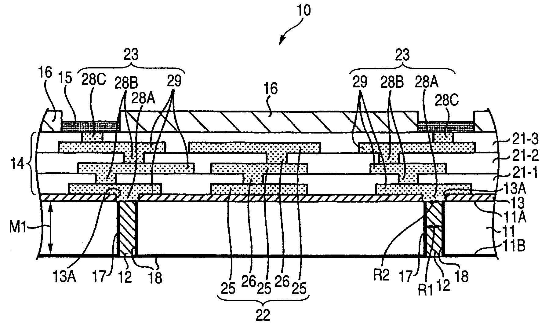
[0048]FIG. 1 is a sectional view of a semiconductor chip according to an embodiment of the present invention.
[0049] Referring to FIG. 1, a semiconductor chip 10 includes a plurality of semiconductor elements (not shown) each of which consists of a semiconductor substrate 11, through vias 12, insulating films 13, 18, a multi-layered wiring structure 14, external connection terminals 15, a protection film 16, transistors, and the like.
[0050] The semiconductor substrate 11 is thinned, and through holes 17 used to provide the through vias 12 are formed in the semiconductor substrate 11. As the semiconductor substrate 11, a silicon substrate can be employed by way of example. Also, as the semiconductor substrate 11, a compound semiconductor such as GaAs, or the like may be employed other than the silicon substrate. A thickness M1 of the semiconductor substrate 11 can be set t...
PUM
 Abstract
Description
Claims
Application Information