
Delay locked loop circuit

Inactive Publication Date: 2007-01-04
SK HYNIX INC
View PDF15 Cites 27 Cited by
  • Summary
  • Abstract
  • Description
  • Claims
  • Application Information

AI Technical Summary

Benefits of technology

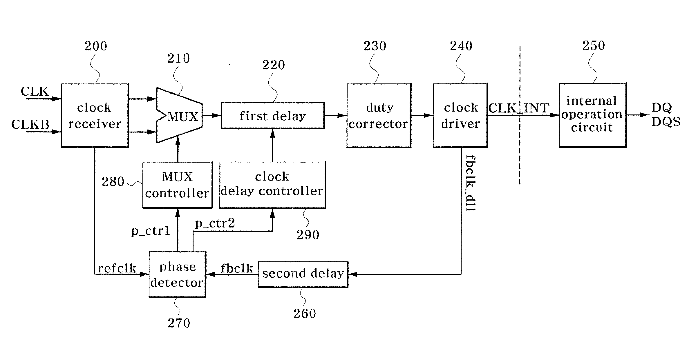
[0015] In accordance with the present patent, the above can be accomplished by the provision of a delay locked loop circuit comprising: a clock receiver for inputting an external clock and outputting an inverted clock and a reference clock, the inverted clock being an inverted version of the external clock; a multiplexer for receiving the external clock and the inverted clock and selectively outputting any one of the received clocks; a first delay for delaying an output signal from the multiplexer by a first desired delay period; a clock driver for receiving an output signal from the first delay and generating an internal clock; a second delay for delaying an output signal from the clock driver by a second desired delay period to output a feedback clock; and a phase detector for comparing a phase of the feedback clock from the second delay with that of the reference clock from the clock receiver and outputting a

Problems solved by technology

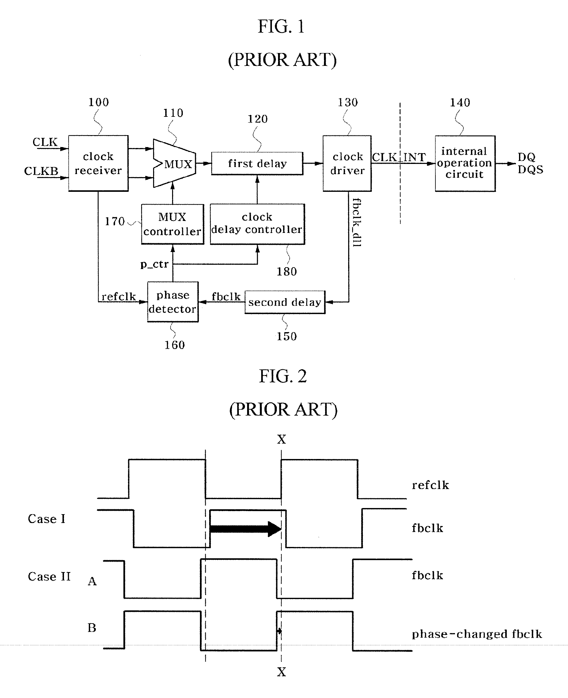
Meanwhile, when an external clock is used within the system, a time delay (clock skew) may occur by an internal circuit of the system.
However, the above-mentioned conventional DLL circuit is disadvantageous in that an error may occur in clock synchronization when the phase of the feedback clock fbclk suffers a change under the influence of system environments, etc.
However, in the initial operation of the DLL circuit, the delay period of the first delay 120 is reduced within a limited range, thereby making it impossible to pull the phase of the feedback clock fbclk forward such that it is aligned with the phase of the reference clock refclk.
For this reason, an error may take place in the synchronization between the feedback clock fbclk and the reference clock refclk, resulting in occurrence of an error in synchronization between the external clock CLK and the DQ strobe.

Method used


Image

  • Delay locked loop circuit
  • Delay locked loop circuit
  • Delay locked loop circuit

Examples


Embodiment Construction

[0032] Reference will now be made in detail to the various embodiments of the present patent, examples of which are illustrated in the accompanying drawings, wherein like reference numerals refer to like elements throughout. The embodiments are described below to explain the present patent by referring to the figures.

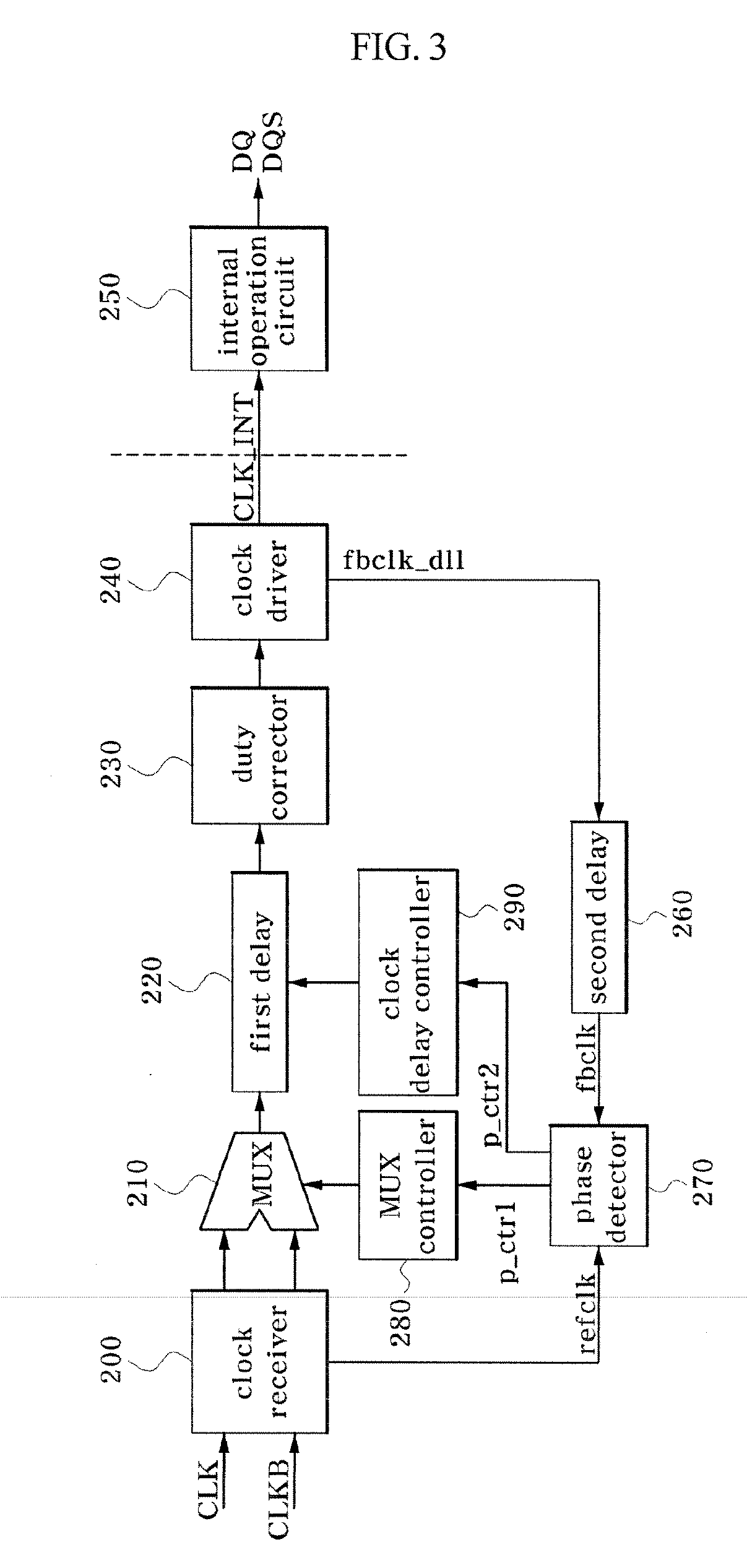
[0033]FIG. 3 shows the configuration of an exemplary delay locked loop (DLL) circuit, FIG. 4 shows the configuration of an exemplary phase detector in the DLL circuit, and FIG. 5 illustrates the exemplary operation characteristics of the DLL circuit. The present patent will hereinafter be described with reference to these figures.

[0034] As shown in FIG. 3, the exemplary DLL circuit includes a clock receiver 200 for receiving an external clock CLK and outputting an inverted clock CLKB and a reference clock refclk, the inverted clock CLKB being an inverted version of the external clock CLK; a multiplexer (MUX) 210 for receiving the external clock CLK and the inverted cl...


PUM


Abstract

A delay locked loop circuit is disclosed. The circuit comprises a clock receiver for outputting an external clock, an inverted clock, which is an inverted version of the external clock, and a reference clock, a multiplexer for receiving the external clock and the inverted clock and selectively outputting any one of the received clocks, a first delay for delaying an output signal from the multiplexer by a first desired delay period, a clock driver for receiving an output signal from the first delay and generating an internal clock, a second delay for delaying an output signal from the clock driver by a second desired delay period to output a feedback clock, and a phase detector for comparing a phase of the feedback clock from the second delay with that of the reference clock from the clock receiver and outputting a first phase control signal for control of a selection operation of the multiplexer and a second phase control signal for control of a delay operation of the first delay in accordance with a result of the comparison.

Description

FIELD OF THE INVENTION [0001] This application relies for priority upon Korean Patent Application No.: 2005-57358 filed on Jun. 29, 2005, the contents of which are herein incorporated by reference in their entirety. The present patent relates to a delay locked loop circuit, and more particularly to a delay locked loop circuit for adjusting the phase of an internal clock, which is the output of the delay locked loop circuit, to such a proper value that the phase of DQ data or a DQ strobe can be synchronized with that of an external clock. DESCRIPTION OF THE RELATED ART [0002] In general, a clock is used in a system or circuit as a reference signal for timing the operation of the system or circuit. The clock may be used to ensure a faster errorless operation of the system or circuit. Meanwhile, when an external clock is used within the system, a time delay (clock skew) may occur by an internal circuit of the system. A phase locked loop (PLL) or delay locked loop (DLL) is generally use...

Claims


Application Information

Patent Timeline
IPC IPC(8): H03L7/06
CPCH03L7/0814H03L7/10H03L7/091H03L7/0816H03L7/08H03L7/089
Inventor NA, KWANG JIN
Owner SK HYNIX INC
Learn More