

Electrostatic discharge protection semiconductor structure
- Summary
- Abstract
- Description
- Claims
- Application Information
AI Technical Summary
Benefits of technology
Problems solved by technology
Method used
Image

Examples
Embodiment Construction
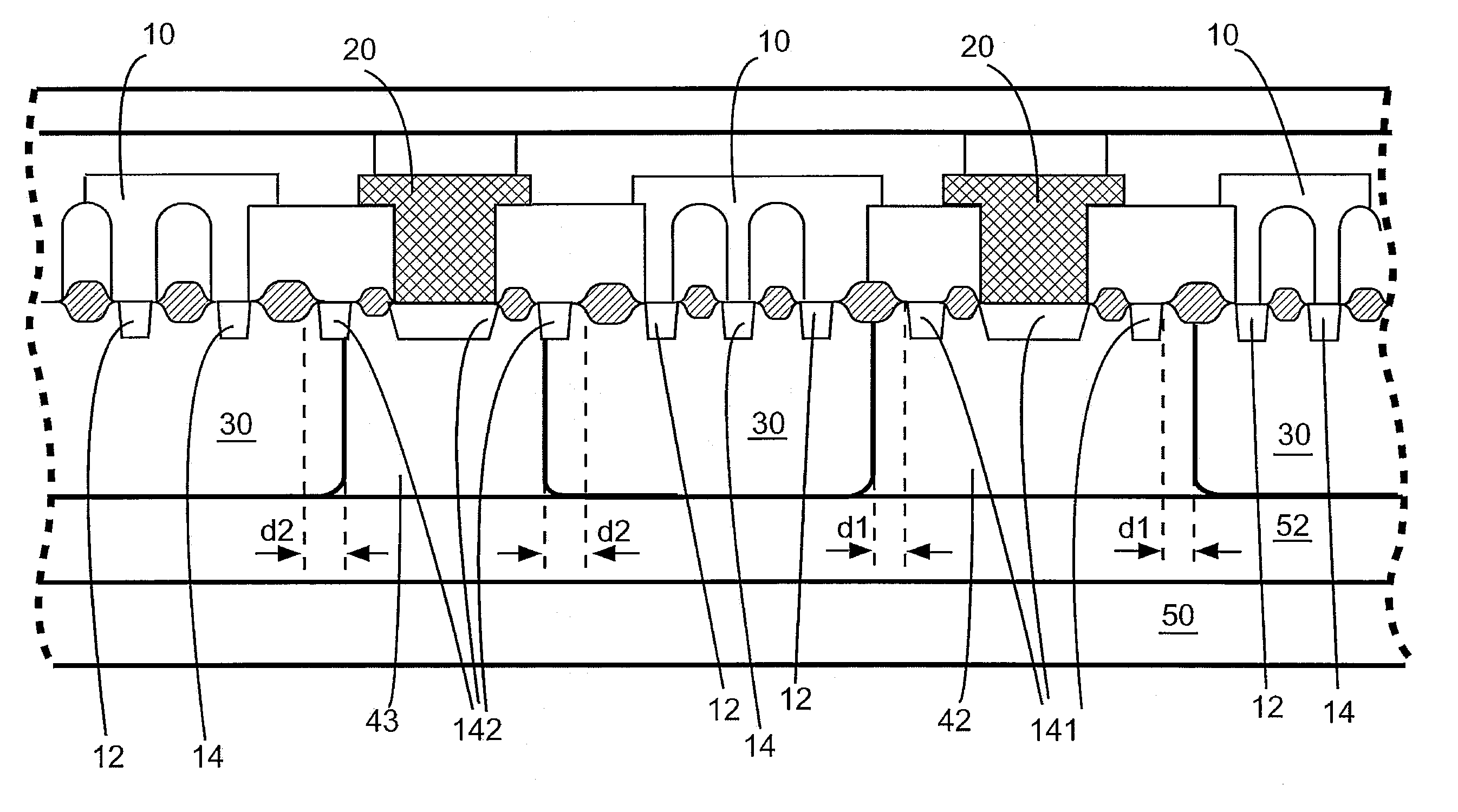
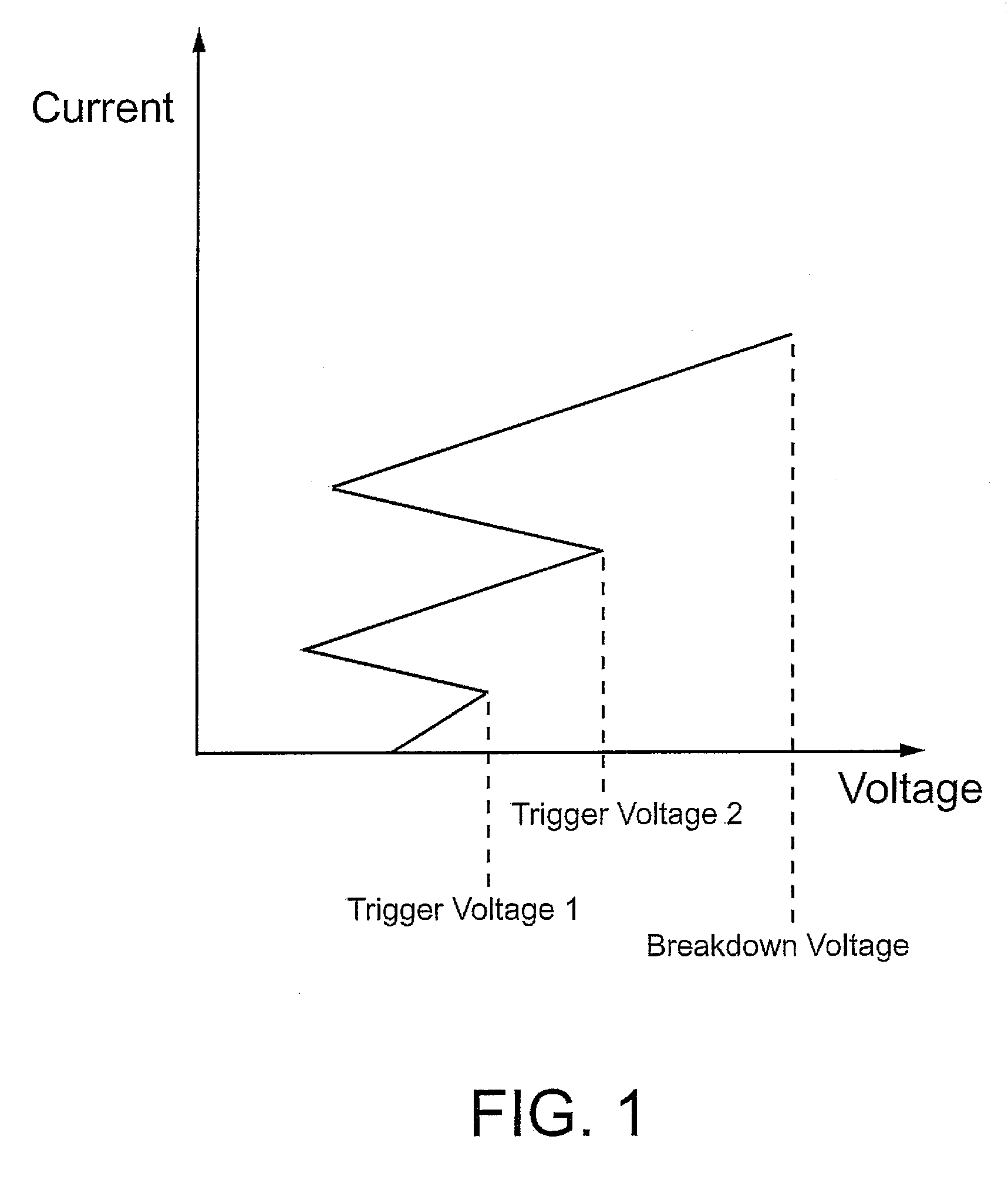
[0018]FIG. 1 is the current-voltage characteristic diagram of the invention. FIGS. 2˜3 are diagrams illustrating the embodiments of the present invention, wherein a plurality of N-wells or P-wells are used to form a particular impedance corresponding to a particular voltage in the P-substrate so as to form an adjustable trigger voltage, and to connect various wells in parallel and make the discharge capacities of various wells to be adjustable, so as to form the multi-trigger ESD protection semiconductor structure.
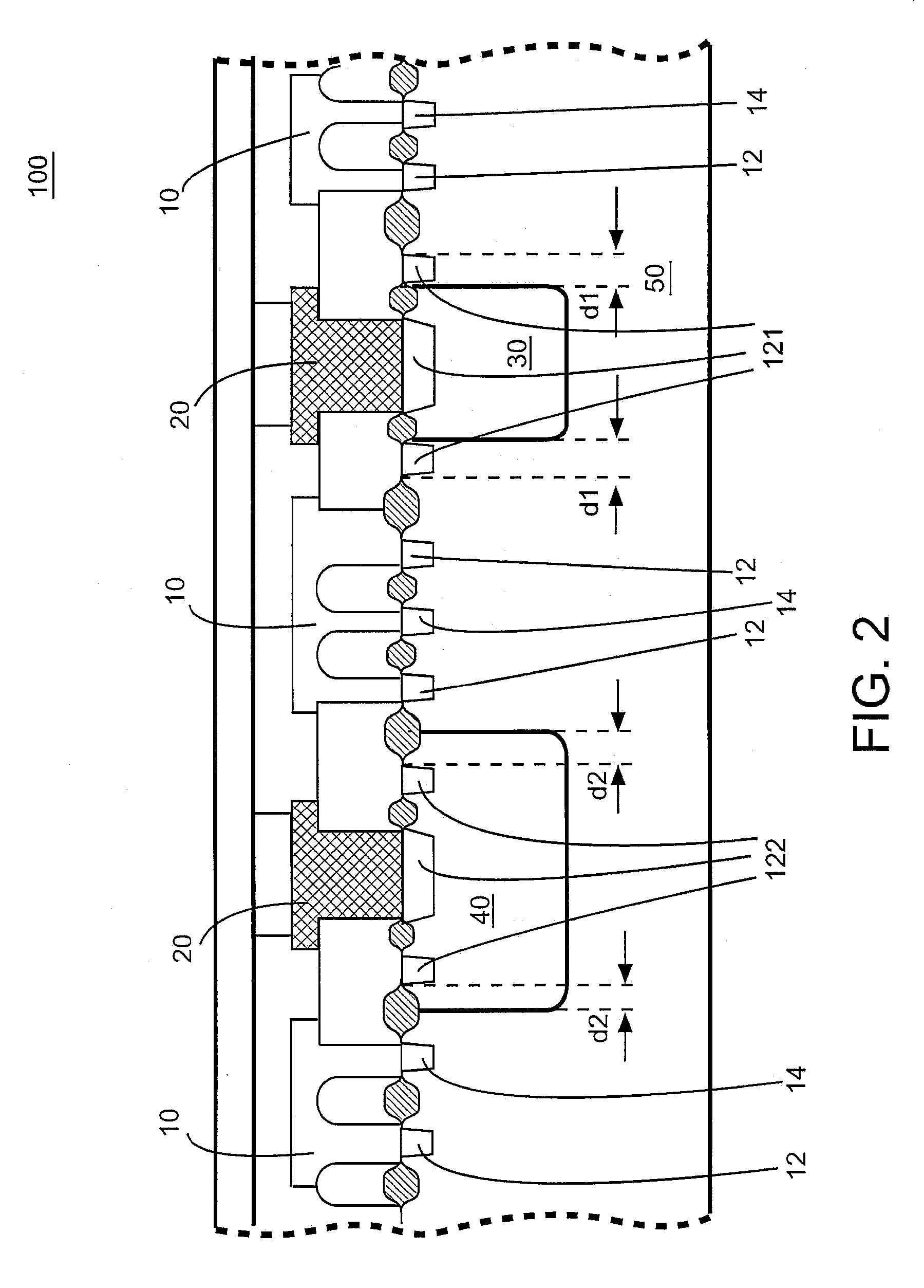
[0019] Referring to the embodiments of the present invention as shown in FIG. 2 and FIG. 3, wherein the embodiment in FIG. 2 includes: a P-substrate 50 having a plurality of ESD protection devices formed thereon (the semiconductor can be implemented with logic device or optoelectronic device, such as transistors or MOS and CMOS devices used for power protection); a first N-well 30 (can be more than one such that a second N-well 40 may be of different impedance) disposed a...
PUM
 Abstract
Description
Claims
Application Information