Semiconductor processing methods

Inactive Publication Date: 2007-01-04
LI WEIMIN +1
View PDF99 Cites 0 Cited by
  • Summary
  • Abstract
  • Description
  • Claims
  • Application Information

AI Technical Summary

Benefits of technology

[0007] In one aspect, the invention encompasses a semiconductor processing method wherein a layer of material is formed over a semiconductive wafer substrate. Some portions of the layer are exposed to energy while other portions are not exposed. The exposure to energy alters physical properties of the exposed portions relative to the unexposed portions. After the portions are exposed, the exposed and unexposed portions of the layer are subjected to common conditions. The common conditions are effective to remove the material and comprise a rate of removal that is influenced by the altered physical properties of the layer. The common conditions remove either the exposed or unexposed portions faster than the other of the exposed and unexposed portions. After the selective removal of the exposed o

Problems solved by technology

Among the reasons for removal of the photoresist is that the photoresist

Method used


Image

  • Semiconductor processing methods
  • Semiconductor processing methods
  • Semiconductor processing methods

Examples


Example

[0018] This disclosure of the invention is submitted in furtherance of the constitutional purposes of the U.S. Patent Laws “to promote the progress of science and useful arts” (Article 1, Section 8).

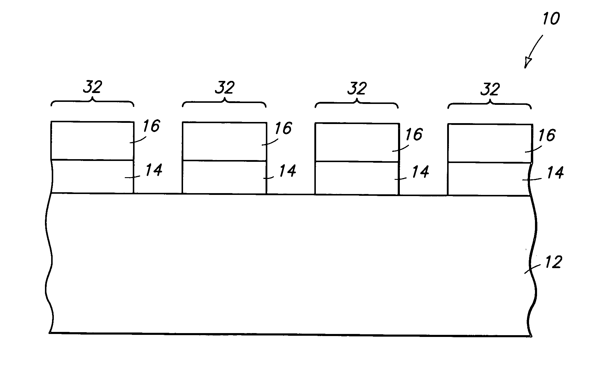
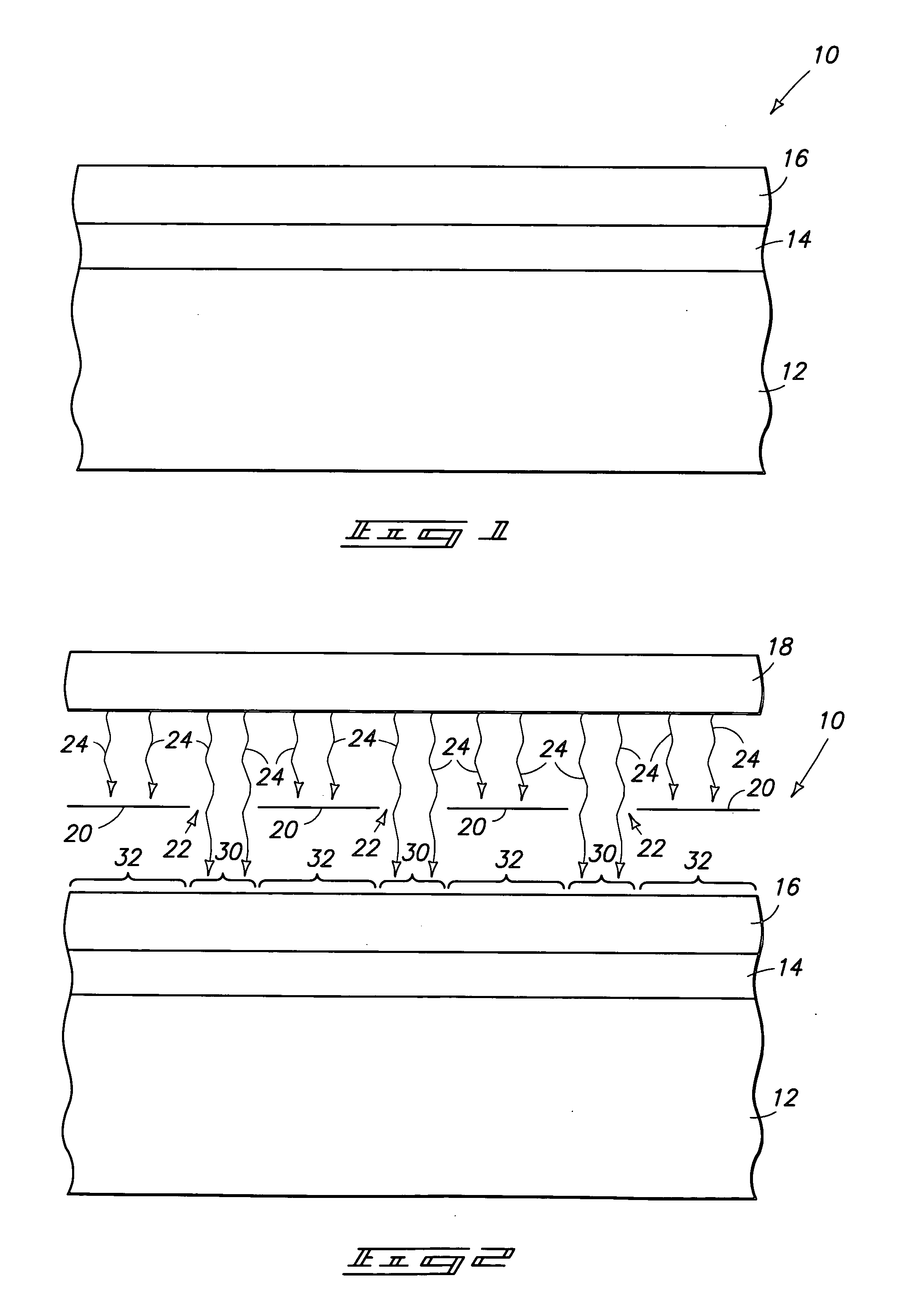
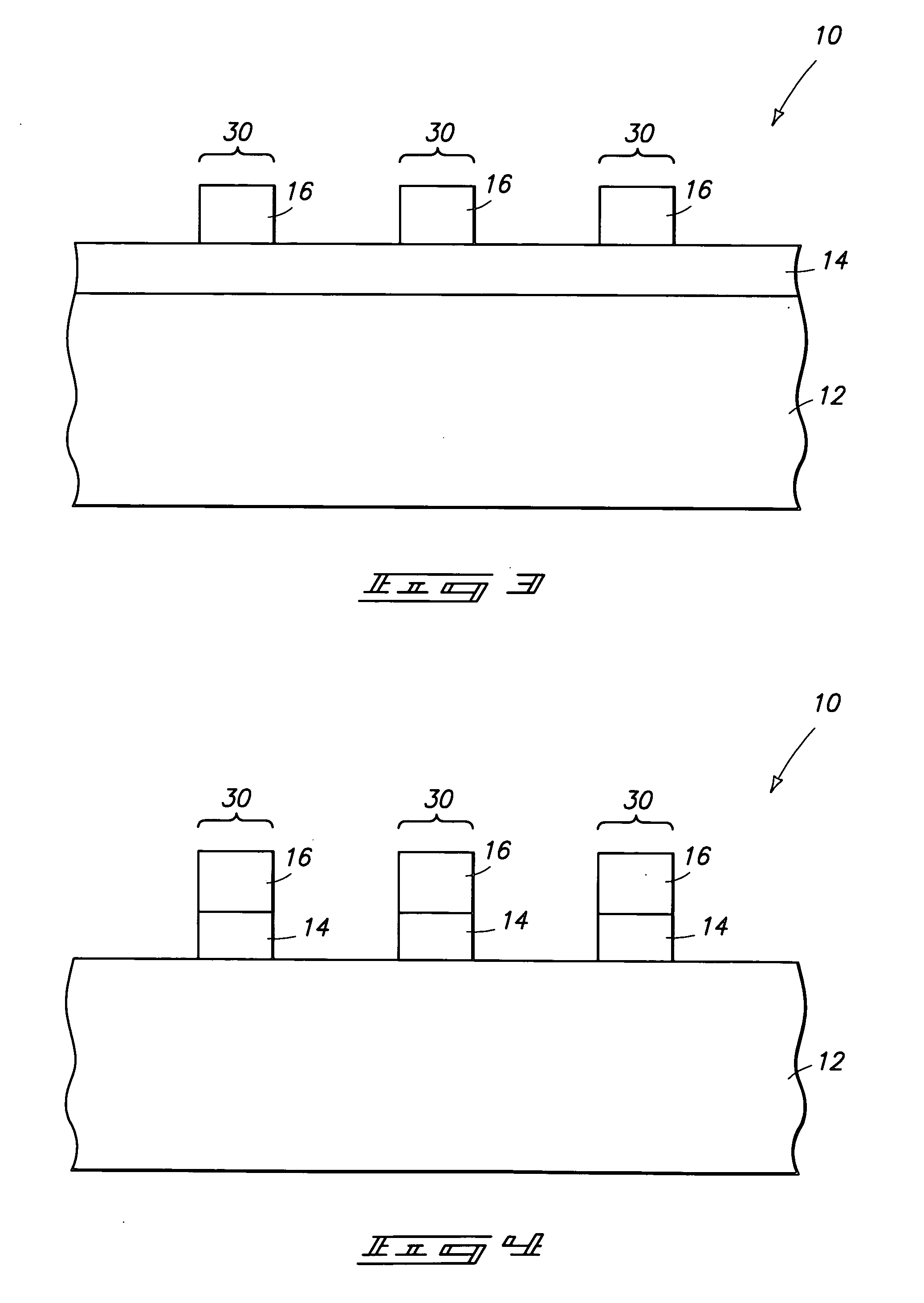
[0019] The invention encompasses methods for utilizing energy to form patterned masking materials on a wafer. In particular aspects of the invention, the patterned masking materials are retained on a wafer after a die-cutting process. In other particular aspects of the invention, the patterned masking materials comprise silicon. The invention is described with reference to a preferred embodiment in FIGS. 1-8.

[0020] Referring to FIG. 1, a semiconductive wafer fragment 10 is illustrated at a preliminary step of a processing sequence encompassed by the present invention. Wafer fragment 10 comprises a semiconductive substrate 12. Substrate 12 can comprise, for example, monocrystalline silicon lightly doped with a p-type conductivity enhancing dopant. To aid in interpretation of the claims ...


PUM


Abstract

In one aspect, the invention encompasses a semiconductor processing method. A layer of material is formed over a semiconductive wafer substrate. Some portions of the layer are exposed to energy while other portions are not exposed. The exposure to energy alters physical properties of the exposed portions relative to the unexposed portions. After the portions are exposed, the exposed and unexposed portions of the layer are subjected to common conditions. The common conditions are effective to remove the material and comprise a rate of removal that is influenced by the altered physical properties of the layer. The common conditions remove either the exposed or unexposed portions faster than the other of the exposed and unexposed portions. After the selective removal of the exposed or unexposed portions, and while the other of the exposed and unexposed portions remains over the substrate, the wafer is cut into separated die. In another aspect, the invention encompasses another semiconductor processing method. A layer of (CH3)ySi(OH)4-y is formed over a substrate. Some portions of the layer are exposed to ultraviolet light while other portions are not exposed. The exposure to ultraviolet light converts the exposed portions to (CH3)xSiO2-x. After the exposure to ultraviolet light, the exposed and unexposed portions of the layer are subjected to hydrofluoric acid to selectively remove the (CH3)ySi(OH)4-y of the unexposed portions relative to the (CH3)xSiO2-x of the exposed portions.

Description

TECHNICAL FIELD [0001] The invention pertains to semiconductor processing methods, and particularly pertains to methods of removing some portions of a layer from over a semiconductive substrate, while leaving other portions of the layer remaining over the substrate. BACKGROUND OF THE INVENTION [0002] Modern semiconductor processing frequently involves photolithographic methods to pattern materials into very small structures, which are ultimately incorporated into a semiconductor circuit. An exemplary prior art method for forming small structures from a layer of material is as follows. First, the layer of material is provided over a semiconductive substrate. Subsequently, a layer of photoresist is provided over the layer of material. A photolithographic mask is then provided over the layer of photoresist and light is shined through the mask to expose portions of the layer of photoresist while leaving other portions unexposed. The photoresist typically comprises an unsaturated organic...

Claims


Application Information

Patent Timeline
IPC IPC(8): H01L21/31
CPCH01L21/02126H01L21/02164H01L21/02271H01L21/78H01L21/31608H01L21/31633H01L21/02348
Inventor LI, WEIMINLI, JOHN Q.
Owner LI WEIMIN
Why Eureka
Try Eureka