

Micromechanical structure, device including the structure, and methods of forming and using same
- Summary
- Abstract
- Description
- Claims
- Application Information
AI Technical Summary
Benefits of technology
Problems solved by technology
Method used
Image

Examples
Embodiment Construction
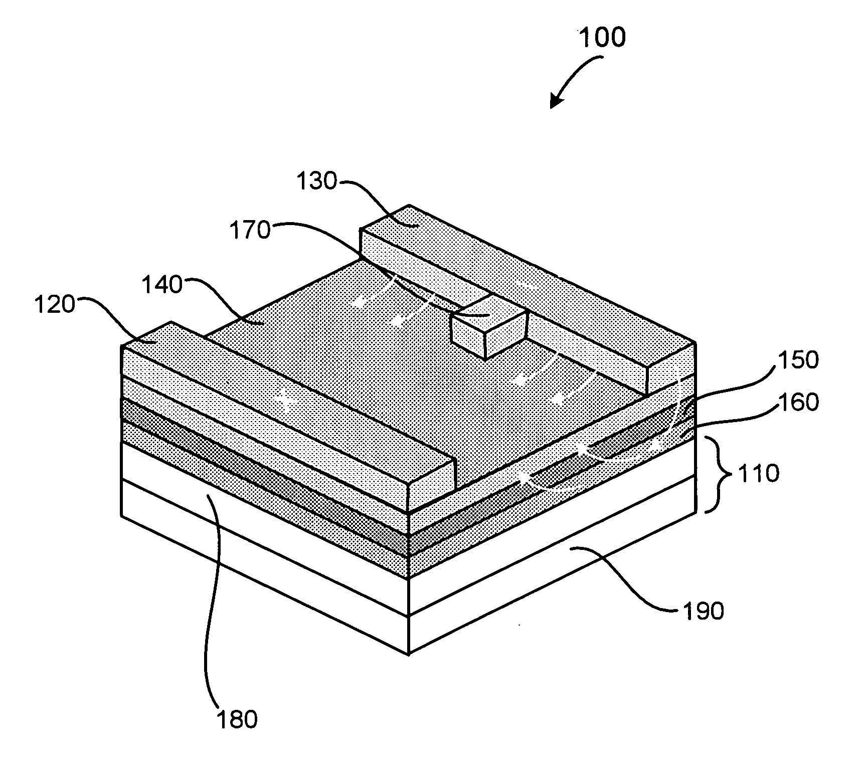
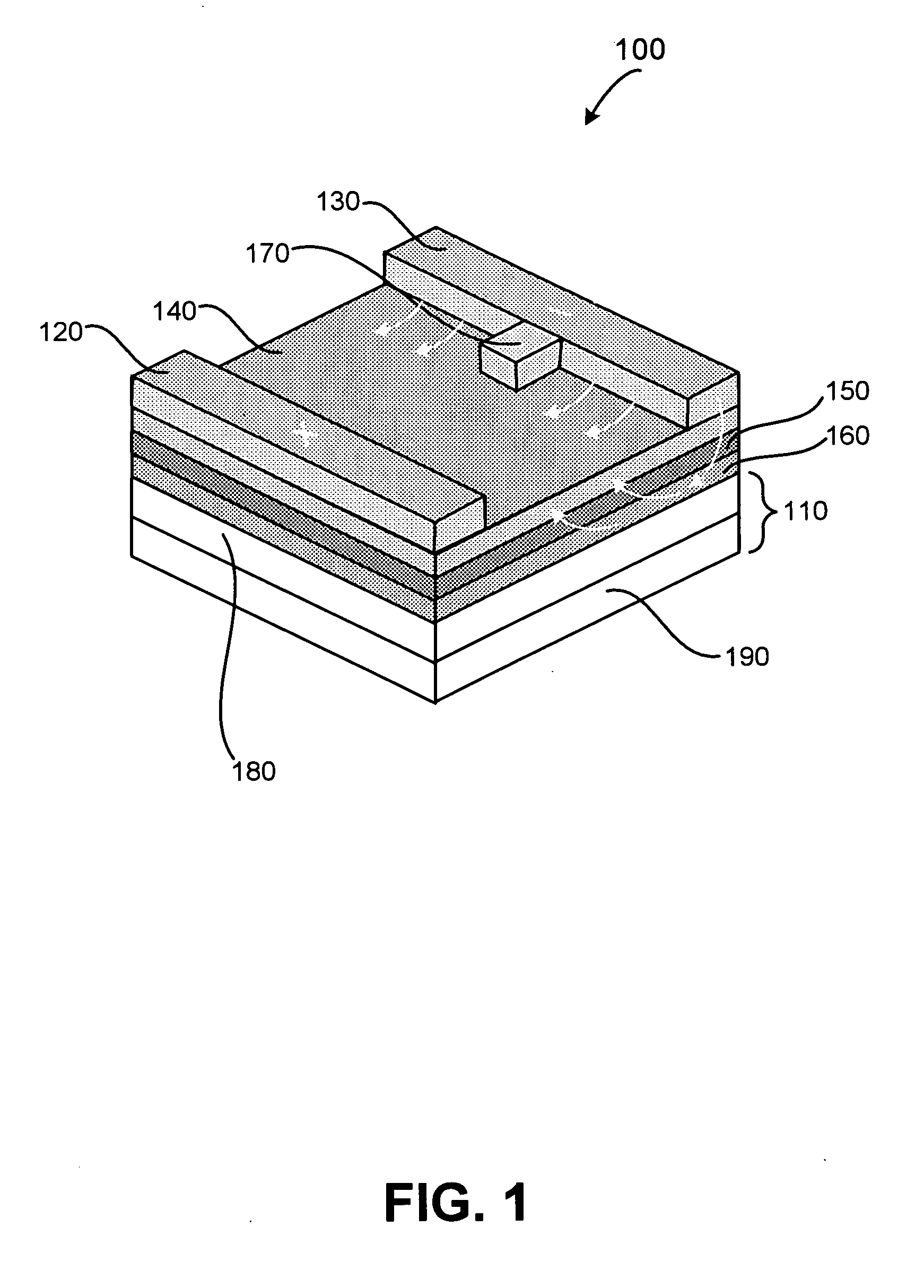
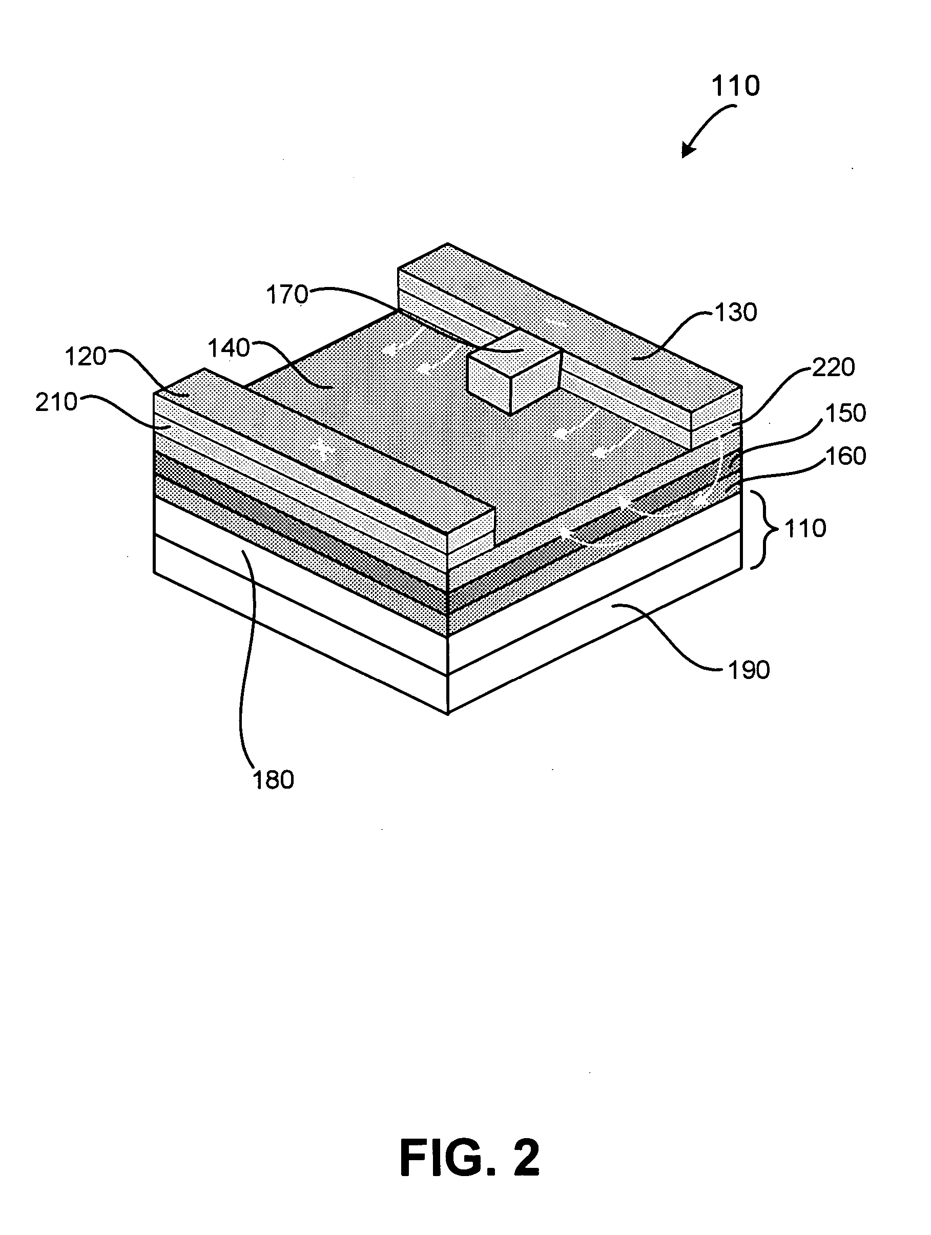
[0019]FIG. 1 illustrates a micromechanical structure 100 formed on a surface of a substrate 110 in accordance with an exemplary embodiment of the present invention. Structure 100 includes electrodes 120 and 130, an ion conductor 140, and optionally includes buffer or barrier layer 150 and / or conducting layer 160. As will be discussed in greater detail below, structure 100 can be used to form devices such as actuators, air-gap switches, and the like. Moreover, because structure 100 can be formed overlying a substrate, the structure allows for monolithic integration of single components and arrays of the structures described herein with electronic, MEMS, or similar devices.
[0020] Generally, structure 100 is configured such that when a bias greater than a threshold voltage (VT), discussed in more detail below, is applied across electrodes 120 and 130, conductive material within ion conductor 140 migrates and thus alters a physical property of structure 100. For example, as a voltage V...
PUM
 Abstract
Description
Claims
Application Information