Communication semiconductor integrated circuit device and wireless communication system

a technology of integrated circuits and semiconductors, applied in the direction of digital transmission, pulse automatic control, transmission, etc., can solve the problem of troublesome time control and achieve the effect of accurate pulling in

Inactive Publication Date: 2007-01-11
RENESAS ELECTRONICS CORP
View PDF11 Cites 16 Cited by
  • Summary
  • Abstract
  • Description
  • Claims
  • Application Information

AI Technical Summary

Benefits of technology

[0007] In a portable telephone, a frequency used is determined at the start of transmitting / receiving operation, a VCO is started, and pull-in control is performed so that a PLL circuit oscillates at the frequency. The pull-in is desired to be performed in short time. In the publication, the pull-in control of the PLL circuit is not disclosed.
[0010] Another object of the invention is to provide a communication semiconductor integrated circuit device capable of pulling in the frequency of a PLL circuit into a desired set frequency accurately at high speed even in the case where a frequency settable range of the PLL circuit is wide.
[0011] Further another object of the invention is to provide a communication semiconductor integrated circuit device capable of performing communication with signals in a plurality of frequency bands and realizing the reduced number of components by forming a VCO on the same semiconductor chip.
[0015] According to the means, an initial voltage extremely close to the control voltage applied when the oscillation circuit oscillates at a desired frequency can be applied at the start of oscillation operation. Thus, a communication semiconductor integrated circuit device having a PLL circuit capable of accurately performing pull-in at high speed without requiring a current source for pull-in of a PLL is obtained.

Problems solved by technology

However, the pull-in method has problems such that a current source for increasing the current at the time of pull-in is necessary in addition to a current source for charging / discharging a charge pump in normal operation.
When the frequency settable range of the PLL circuit is wide, troublesome time control is necessary to accurately pull the frequency of the PLL circuit into a desired set frequency.

Method used


Image

  • Communication semiconductor integrated circuit device and wireless communication system
  • Communication semiconductor integrated circuit device and wireless communication system
  • Communication semiconductor integrated circuit device and wireless communication system

Examples


Embodiment Construction

[0023] Embodiments of the invention will be described hereinbelow with reference to the drawings.

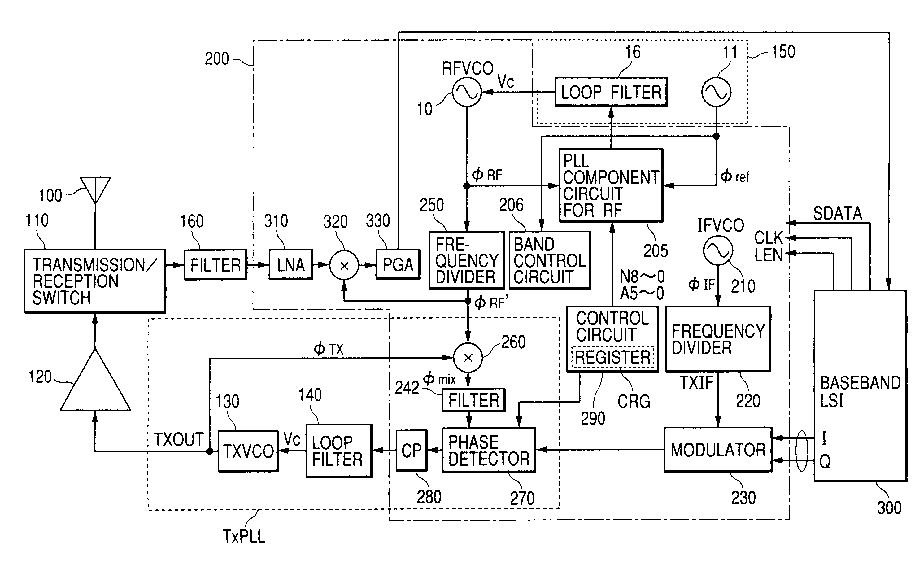
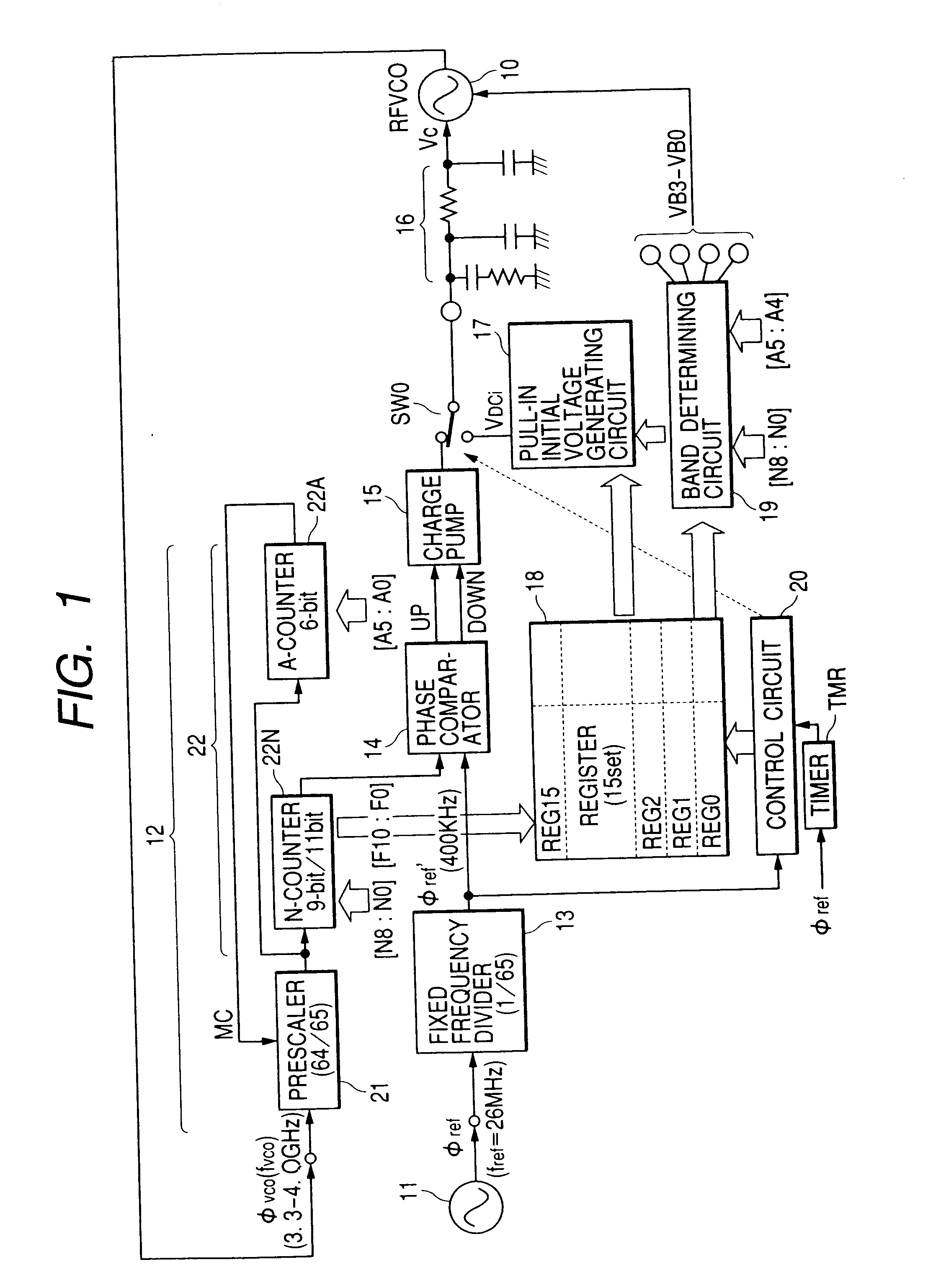
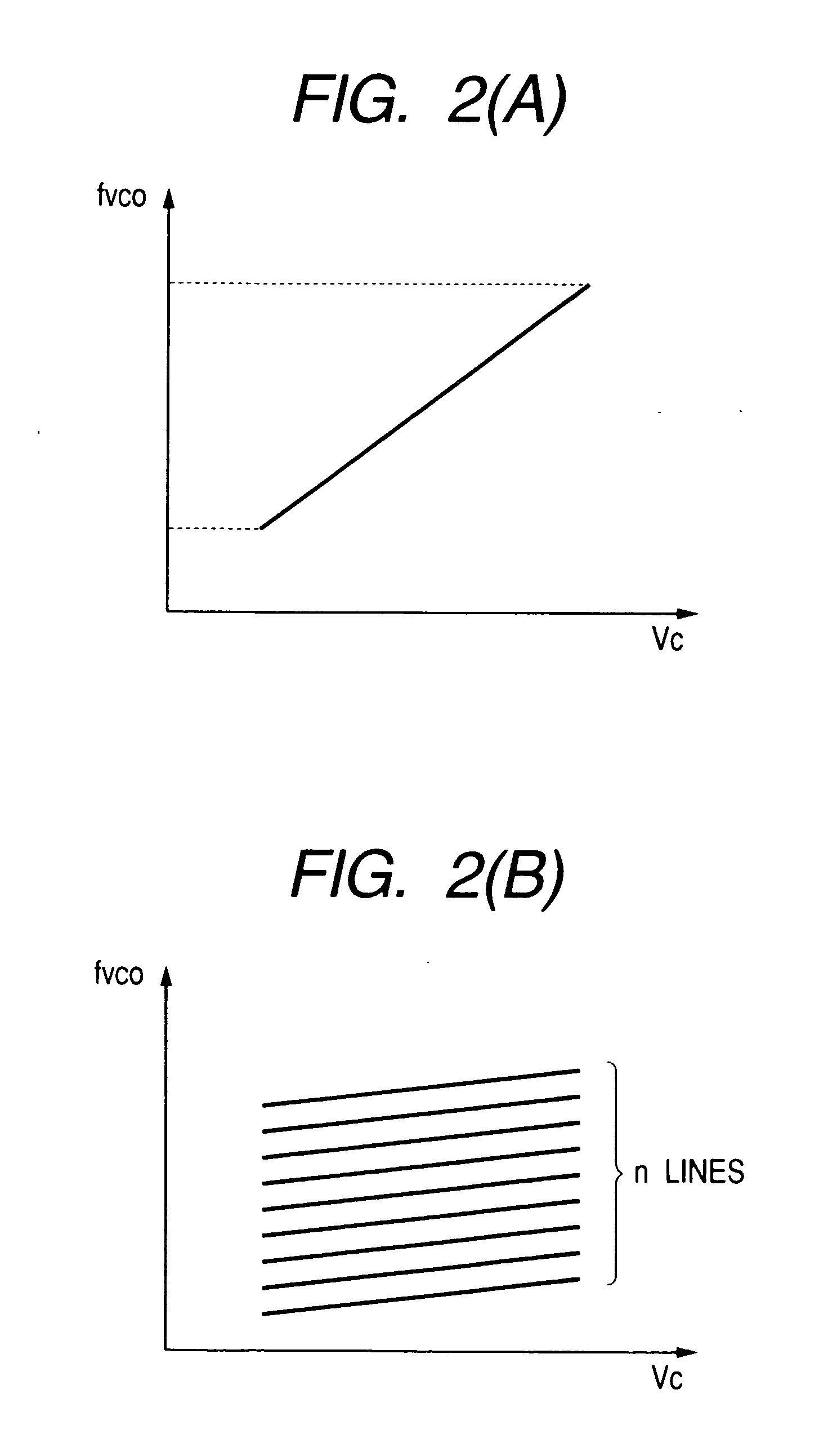
[0024]FIG. 1 shows an example of a high-speed pull-in PLL circuit to which the invention is applied. Shown in the diagram are a VCO (Voltage Controlled Oscillator) 10, a reference oscillation circuit (TCXO) 11 which uses a crystal oscillator and oscillates at precise high frequencies, a variable frequency divider 12 for dividing the frequency of an oscillation signal φvco of the VCO 10, a fixed frequency divider 13 for dividing the frequency of a reference oscillation signal φref of the reference oscillation circuit 11 to 1 / 65, a phase comparator 14 for comparing the phase of a signal subjected to frequency division of the variable frequency divider 12 with the phase of signal subjected to frequency division of the fixed frequency divider 13 and outputting a voltage UP or DOWN according to a phase difference, a charge pump 15, and a loop filter 16. A PLL loop in which the capacitive ele...


PUM


Abstract

The invention provides a communication semiconductor integrated circuit device (RF IC) capable of pulling in the frequency of a PLL circuit to a desired set frequency at high speed even in the case where a frequency settable range of the PLL circuit is wide without providing a current source other than a current source for charging and discharging in an normal operation. An oscillator as a component of a PLL circuit is constructed so as to be operative in a plurality of bands. In a state where a control voltage of the oscillator is fixed to a predetermined value, an oscillation frequency of the oscillator is measured in each of bands and stored in a storing circuit. A set value for designating a band supplied at the time of PLL operation is compared with the stored measured frequency value. From a result of comparison, a band to be actually used in the oscillator is determined, and a frequency difference between the maximum frequency of the selected band and the set frequency is obtained. Further, a control voltage closest to the set frequency is determined on the basis of the frequency difference and the frequency variable range of the selected band and the control voltage is applied to the oscillator to start oscillating operation. After that, a PLL loop is closed and locked.

Description

BACKGROUND OF THE INVENTION [0001] The present invention relates to a technique effective to be applied to a PLL (Phase Locked Loop) circuit having a VCO (Voltage Controlled Oscillator) and capable of switching an oscillation frequency and further to a high-speed pull-in technique of a PLL circuit. More particularly, the invention relates to a technique effective to be applied to a PLL circuit for generating an oscillation signal of a predetermined frequency mixed with a reception signal or transmission signal in a radio communication device such as a portable telephone capable of transmitting / receiving signals in a plurality of bands, a semiconductor integrated circuit device for high frequencies having the same, and a radio communication system. [0002] In a radio communication system such as a portable telephone, a PLL circuit is used as a local oscillator for generating an oscillation signal of a predetermined frequency mixed with a reception signal or transmission signal. Hither...

Claims


Application Information

Patent Timeline
Patent Type & Authority Applications(United States)
IPC IPC(8): H04B1/40H04B1/06H03L7/187H03L7/089H03L7/099H03L7/10H03L7/183H03L7/189H03L7/193H04B1/3822
CPCH03L7/0891H03L7/193H03L7/10H03L7/107H03L7/101H03L7/00
Inventor OOSAWA, HIROTAKAKASAHARA, MASUMIKURAKAMI, NORIYUKIUOZUMI, TOSHIYA
Owner RENESAS ELECTRONICS CORP
Why Eureka
Try Eureka