Transistor for semiconductor device and method of forming the same

a technology of semiconductor devices and transistors, which is applied in the field of memory devices, can solve the problems of decreasing the yield of the semiconductor device and increasing the product cost, and achieve the effects of increasing the channel length, increasing the channel area, and simplifying the process steps

a technology of semiconductor devices and transistors, which is applied in the field of memory devices, can solve the problems of decreasing the yield of the semiconductor device and increasing the product cost, and achieve the effects of increasing the channel length, increasing the channel area, and simplifying the process steps

US20070012997A1Inactive Publication Date: 2007-01-18SK HYNIX INC

Image

  • Transistor for semiconductor device and method of forming the same
  • Transistor for semiconductor device and method of forming the same
  • Transistor for semiconductor device and method of forming the same

Examples


Embodiment Construction

[0023] Reference will now be made in detail to exemplary embodiments of the present invention. Wherever possible, the same reference numbers will be used throughout the drawings to refer to the same or like parts. It should be appreciated that the embodiments are provided for the purpose that one ordinarily skilled in the art would be able to understand the present invention, and modifications in various manners and the scope of the present invention are not limited by the embodiments described herein.

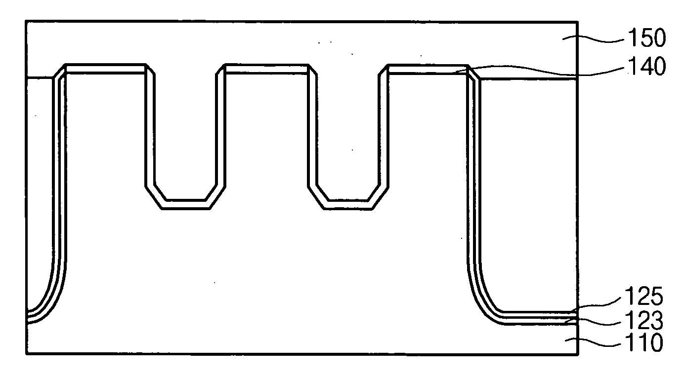
[0024]FIG. 4 is a simplified layout view of a transistor for a semiconductor device according to a first embodiment of the present invention. FIGS. 5A through 5D are simplified cross-sectional views illustrating a method of forming a transistor for a semiconductor device in accordance with a first embodiment of the present invention. In addition, FIGS. 6 and 7 are simplified layout views of a transistor for a semiconductor device in accordance with a second and third embodiments of th...


PUM


Abstract

Disclosed herein is a transistor for a semiconductor device and a method of forming the same. According to the present invention, a recess channel region is formed on a cell region to increase a channel length and a fin-type channel region is simultaneously formed on a peripheral circuit region to increase a channel area so as to simplify process steps, thereby improving the yield and productivity for manufacturing a semiconductor device.

Description

BACKGROUND OF THE INVENTION [0001] 1. Field of the Invention [0002] The present invention relates to a memory device. In particular, the present invention provides a transistor for a semiconductor device and a method of forming the same, and more specifically to a transistor for a semiconductor device and a method of forming the same wherein a recess channel region is formed on a cell region to increase a channel length and a fin-type channel region is simultaneously formed on a peripheral circuit region to increase a channel area so as to simplify process steps, thereby improving the yield and productivity for manufacturing a semiconductor device. [0003] 2. Discussion of the Related Art [0004] Recently, there has been a trend in demanding a transistor having sufficient drive current and lower power in order to increase its operating speed even though design rules of a semiconductor device are reduced. Channel area is one considerable factor for determining drive current a transisto...

Claims


Application Information

Patent Timeline
18 Jan 2007
Publication
US20070012997A1
IPC
H01L29/76; H01L29/94; H01L31/00
CPC
H01L29/7834; H01L29/66621; H01L21/18; H01L21/76
Inventors
CHUNG, SUNG WOONG; LEE, SANG DON