

Integrated circuit device and electronic instrument
a technology of integrated circuits and electronic instruments, applied in the field of integrated circuit devices and electronic instruments, can solve the problems of increasing circuit scale and circuit complexity, reducing the chip area of the driver circuit, and manufacturing costs that cannot be reduced
- Summary
- Abstract
- Description
- Claims
- Application Information
AI Technical Summary
Problems solved by technology
Method used
Image

Examples
Embodiment Construction
[0054] The invention may provide an integrated circuit device which can prevent an erroneous detection by protecting bitlines, even when the degrees of freedom of the layout of the integrated circuit device including a display memory are increased or the size of the integrated circuit device is reduced by providing an interconnect for supplying a relatively high voltage in a layer above the bitlines, and an electronic instrument including the same.
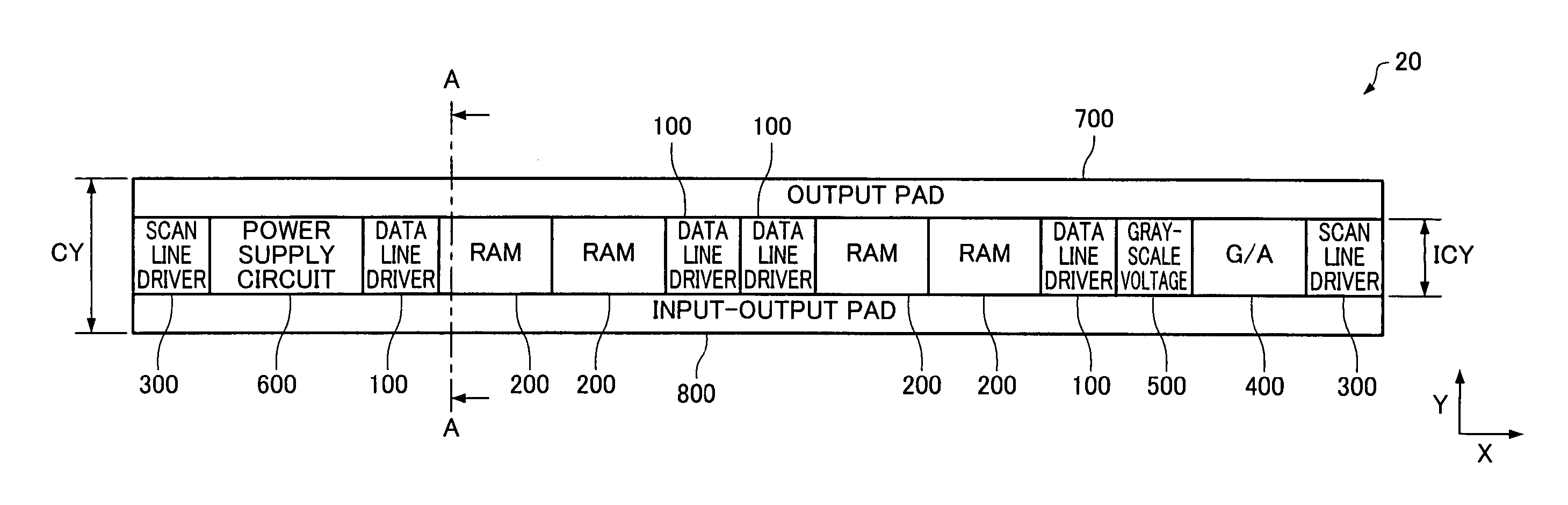
[0055] According to one embodiment of the invention, there is provided an integrated circuit device having a display memory which stores at least part of data displayed in a display panel which has a plurality of scan lines and a plurality of data lines, wherein the display memory includes a plurality of wordlines, a plurality of bitlines, and a plurality of memory cells;
[0056] wherein a plurality of first power supply interconnects for supplying a first power supply voltage to the memory cells are formed in a metal interconnect layer in...
PUM
 Abstract
Description
Claims
Application Information