Liquid crystal display panel and testing and manufacturing methods thereof

Active Publication Date: 2007-01-25
SAMSUNG DISPLAY CO LTD
View PDF6 Cites 60 Cited by
  • Summary
  • Abstract
  • Description
  • Claims
  • Application Information

AI Technical Summary

Benefits of technology

[0012] An aspect of the present invention provides an LCD panel capable of simplifying testing and manufacturing methods thereof, for example, by obviating the conventional shorting bars and the corresponding shorting bar removing process.

Problems solved by technology

During this removing process, a pollutant may occur, or signal lines may corrode due to moisture or other contaminants injected through a cut surface, thereby degrading reliability.

Method used


Image

  • Liquid crystal display panel and testing and manufacturing methods thereof
  • Liquid crystal display panel and testing and manufacturing methods thereof
  • Liquid crystal display panel and testing and manufacturing methods thereof

Examples


first embodiment

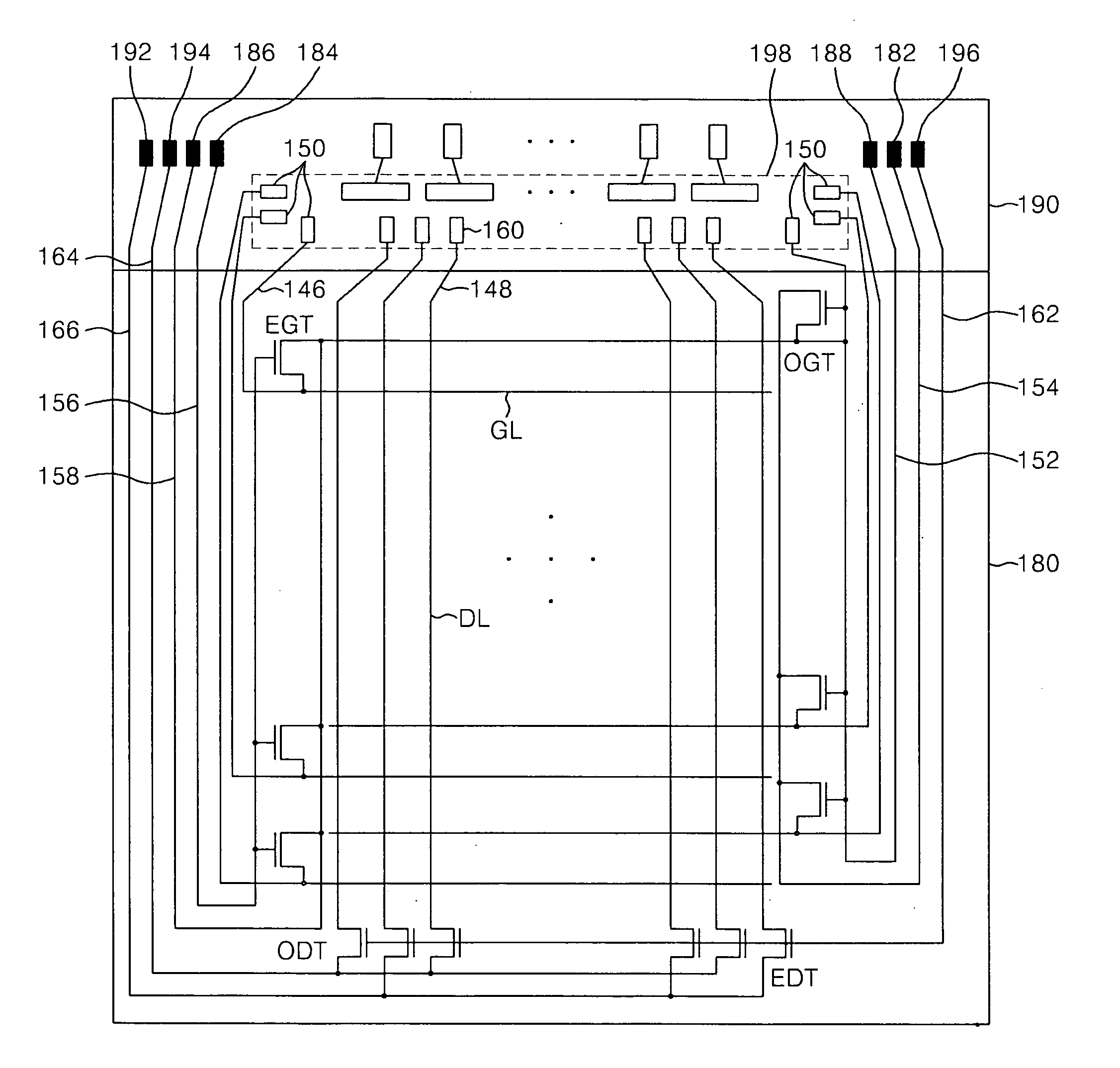
[0045]FIG. 1 is a plane view illustrating an LCD panel according to the present invention.

[0046] The LCD panel shown in FIG. 1 includes a display area 180 and a peripheral area 190. The display area 180 includes a plurality of odd and even data test transistors ODT and EDT connected to data lines DL (DL1, DL2, DL3, DL4, . . . ) (in a display region of the display area 180), and a plurality of odd and even gate test transistors OGT and EGT connected to gate lines GL in the display region. After the testing process if the panel passes, a semiconductor integrated circuit (IC) chip, such as a Driver IC, and / or an IC Package is physically and electrically attached to the substrate in a predetermined package region 198 for receiving the Driver IC package in the non-display (peripheral) region 190. The “package region” receives the Driver IC “package”. In various embodiments, the Driver IC “package” may comprise a Driver IC chip plus a mounting board and plurality of conductive patterns. I...

second embodiment

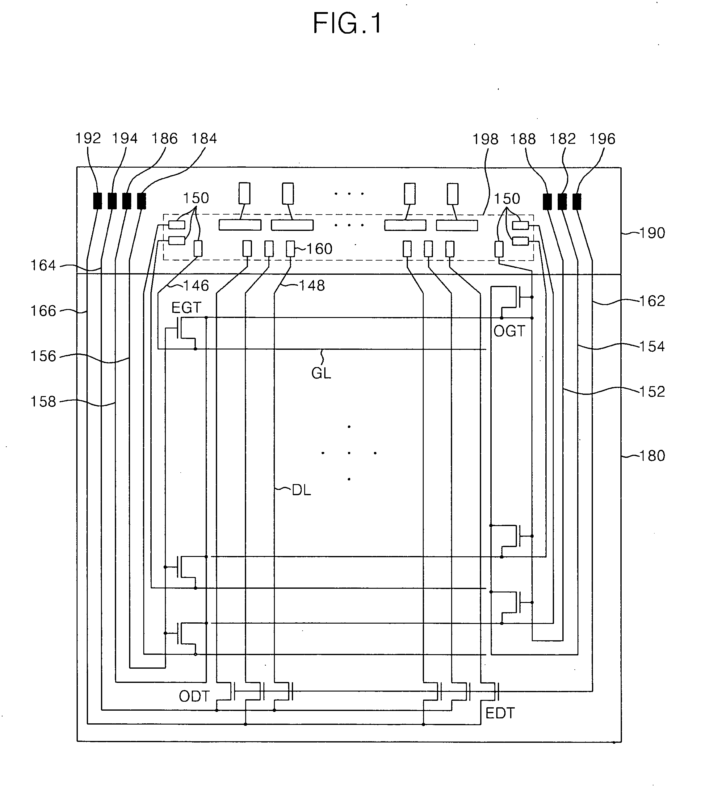
[0053]FIG. 2 is a plane view illustrating an LCD panel according to the present invention. The LCD panel shown in FIG. 2 includes a display area 180 and a peripheral area 190.

[0054] The LCD panel shown in FIG. 2 includes pixel transistors TFT and pixel electrodes PXL formed in pixel regions at the intersections of gate lines GL and data lines DL, odd and even data test transistors ODT and EDT connected to the data lines DL in the display region 168, and odd and even gate test transistors OGT and EGT connected to the gate lines GL in the display region 168.

[0055] The odd data test transistors ODT include respective transistor gate electrodes (connected to a data control pad 196 and line 162), respective transistor source electrodes (connected to an odd data test pad 194 and line 164), and respective drain electrodes (connected through odd data pads 160 to odd data lines DL1, DL3, . . . , DLm-1). The odd data test transistors ODT switchably apply to the odd data lines DL1, DL3, . . ....

third embodiment

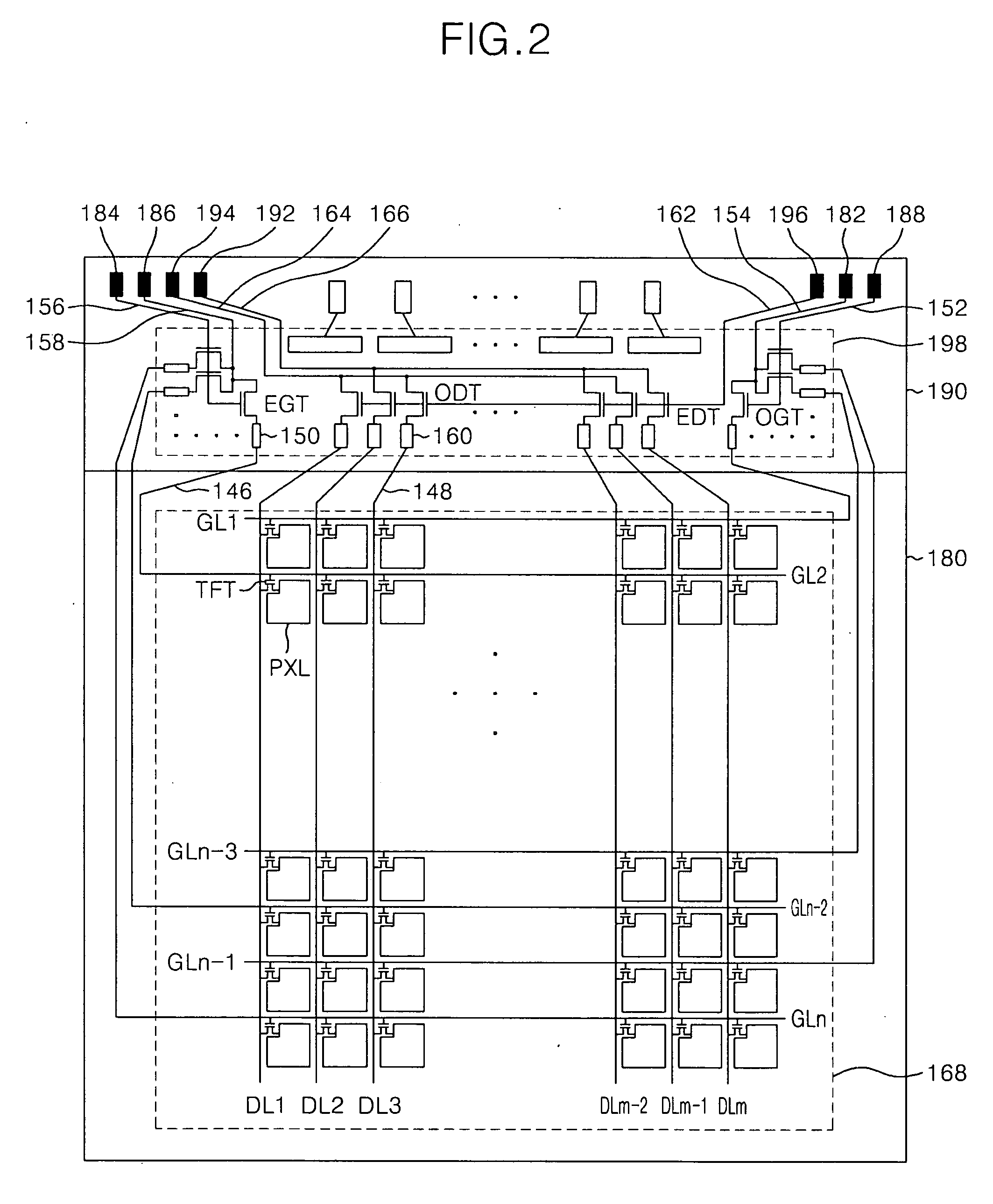
[0071]FIG. 5 is a plane view of an LCD panel according to the present invention. The LCD panel shown in FIG. 5 includes a display area 180 and a peripheral area 190.

[0072] The LCD panel shown in FIG. 5 includes pixel transistors TFT and pixel electrodes PXL (formed in pixel regions defined by the intersections of gate lines GL and data lines DL), odd and even data test transistors ODT and EDT (connected to the data lines DL of a display region 168), and a gate driver 178 connected to the gate lines GL of the display region 168.

[0073] The odd data test transistors ODT include respective transistor gate electrodes (connected to a data control pad 196 and line 162), respective transistor source electrodes (connected to an odd data test pad 194 and line 164), and respective transistor drain electrodes (connected through odd data pads 160 to odd data lines DL1, DL3, . . . , DLm-1). The odd data test transistors ODT switchably transmit to the odd data lines DL1, DL3, . . . , DLm-1 a data...


PUM


Abstract

A liquid crystal display (LCD) panel simplifying its testing and manufacturing. The LCD panel includes (formed on a substrate) gate lines, data lines, and pixels including pixel transistors. The LCD panel further includes a plurality test transistors (e.g., data test transistors for driving the odd and even data lines) formed in a package region of a driving IC (integrated circuit) configured to drive the data lines. The plurality of test transistors may be selectively activated (turned ON) during testing before the driving integrated circuit (Driver IC package) is attached (e.g., fixed) to the driving IC package region. The LCD panel may further include a plurality of gate test transistors configured to drive the odd and even gate lines.

Description

CROSS-REFERENCE TO RELATED APPLICATION [0001] This application claims priority to Korean Patent Application No. 2005-65284 filed on Jul. 19, 2005, the contents of which are hereby incorporated by reference in their entirety. BACKGROUND OF THE INVENTION [0002] 1. Field of the Invention [0003] The present invention relates to a liquid crystal display (LCD) panel, and more particularly, to a LCD panel capable of simplifying testing and manufacturing methods thereof. [0004] 2. Description of the Related Art [0005] A liquid crystal display (LCD) displays images by controlling the light transmittance through a liquid crystal layer by applying an electric field based on received image data signals. The LCD includes an LCD panel in which liquid crystal cells are arrayed in a matrix, and a driving circuit (e.g., disposed in a peripheral area adjacent to the pixel array) for driving the LCD panel based on the received image data signals. [0006] The pixel array of the LCD panel includes a thin...

Claims


Application Information

Patent Timeline
IPC IPC(8): G01R31/00
CPCG09G3/006G09G3/3688G09G3/3677G02F1/133
Inventor JEON, JINJUNG, MIN KYUNG
Owner SAMSUNG DISPLAY CO LTD
Why Eureka
Try Eureka